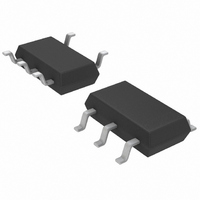
LTC6101HVCHS5#TRMPBF Linear Technology, LTC6101HVCHS5#TRMPBF Datasheet - Page 10

LTC6101HVCHS5#TRMPBF
Manufacturer Part Number
LTC6101HVCHS5#TRMPBF
Description
IC AMP CURRENT SENSE TSOT23-5
Manufacturer
Linear Technology
Datasheet
1.LTC6101HVAHS5TRMPBF.pdf
(20 pages)
Specifications of LTC6101HVCHS5#TRMPBF
Amplifier Type
Current Sense
Number Of Circuits
1
Gain Bandwidth Product
200kHz
Current - Input Bias
100nA
Voltage - Input Offset
400µV
Current - Supply
350µA
Current - Output / Channel
1mA
Voltage - Supply, Single/dual (±)
5 V ~ 100 V
Operating Temperature
0°C ~ 70°C
Mounting Type
Surface Mount
Package / Case
TSOT-23-5, TSOT-5, TSOP-5
Lead Free Status / RoHS Status
Lead free / RoHS Compliant
Output Type
-
-3db Bandwidth
-
Slew Rate
-
Available stocks
Company
Part Number
Manufacturer
Quantity
Price
LTC6101/LTC6101HV
Selection of External Input Resistor, R
The external input resistor, R
tance of the current sense circuit. Since I
transconductance g
I
R
while limiting the output current. At low supply voltage,
I
the largest expected sense voltage gives I
the maximum output dynamic range is available. Output
dynamic range is limited by both the maximum allowed
output current and the maximum allowed output voltage, as
well as the minimum practical output signal. If less dynamic
range is required, then R
reducing the max output current and power dissipation.
If low sense currents must be resolved accurately in a
system that has very wide dynamic range, a smaller R
than the max current spec allows may be used if the max
current is limited in another way, such as with a Schottky
diode across R
current measurement accuracy by limiting the result, while
increasing the low current measurement resolution.
10
APPLICATIONS INFORMATION
OUT
OUT
IN
should be chosen to allow the required resolution
= V
may be as much as 1mA. By setting R
SENSE
V
OUT
I
LOAD
/100 or I
SENSE
+IN
CMPZ4697
301
m
V
–
= 1/R
(Figure 3a). This will reduce the high
10k
LTC6101
OUT
IN
+
R
IN
SENSE LO
= 1mA for V
100m
can be increased accordingly,
. For example, if R
IN
–
, controls the transconduc-
M1
Si4465
Figure 3b. Dual LTC6101s Allow High-Low Current Ranging
301
–IN
OUT
V
+
V
IN
R
7.5k
SENSE
OUT
IN
5
OUT
+IN
301
V
= V
–
IN
IN
= 1mA, then
= 100mV.
LTC6101
= 100, then
SENSE
such that
(
0 ≤ I
V
+
LOGIC
R
SENSE HI
LOAD
10m
–
/R
+5V
≤ 10A
IN
IN
)
,
≤ V
7.5k
–IN
301
V
OUT
IN
+
≤ 60V
Figure 3a. Shunt Diode Limits Maximum Input Voltage to Allow
Better Low Input Resolution Without Overranging
This approach can be helpful in cases where occasional
large burst currents may be ignored. It can also be used
in a multirange confi guration where a low current circuit
is added to a high current circuit (Figure 3b). Note that
a comparator (LTC1540) is used to select the range, and
transistor M1 limits the voltage across R
Care should be taken when designing the board layout
for R
connect impedances will increase the effective R
causing a gain error. In addition, internal device resistance
will add approximately 0.2Ω to R
V
IN
IN,
BAT54C
especially for small R
V
LOGIC
1.74M
619k
40.2k
HIGH CURRENT RANGE OUT
250mV/A
LOW CURRENT RANGE OUT
2.5V/A
3
4
5
6
(3.3V TO 5V)
R
+
–
SENSE
V
2
LOGIC
7
1
LOAD
LTC1540
V
+
6101 F03a
(I
INDICATOR
LOAD
IN
8
RANGE
HIGH
values. All trace and inter-
> 1.2A)
D
IN
SENSE
6101 F03b
.
4.7k
SENSE LO
Q1
CMPT5551
IN
.
value,
6101fg


