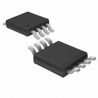
LTC1992CMS8#TRPBF Linear Technology, LTC1992CMS8#TRPBF Datasheet - Page 3

LTC1992CMS8#TRPBF
Manufacturer Part Number
LTC1992CMS8#TRPBF
Description
IC AMP/DVR I/O FULLY DIFF 8-MSOP
Manufacturer
Linear Technology
Datasheet
1.LTC1992CMS8PBF.pdf
(42 pages)
Specifications of LTC1992CMS8#TRPBF
Amplifier Type
Differential
Number Of Circuits
1
Output Type
Differential, Rail-to-Rail
Slew Rate
1.5 V/µs
Gain Bandwidth Product
3.2MHz
Current - Input Bias
2pA
Voltage - Input Offset
250µV
Current - Supply
700µA
Current - Output / Channel
30mA
Voltage - Supply, Single/dual (±)
2.7 V ~ 11 V, ±1.35 V ~ 5.5 V
Operating Temperature
0°C ~ 70°C
Mounting Type
Surface Mount
Package / Case
8-MSOP, Micro8™, 8-uMAX, 8-uSOP,
Lead Free Status / RoHS Status
Lead free / RoHS Compliant
-3db Bandwidth
-
Available stocks
Company
Part Number
Manufacturer
Quantity
Price
elecTrical characTerisTics
temperature range, otherwise specifications are at T
noted. V
defined as (+V
SYMBOL
V
I
V
∆V
PSRR
GCM
V
∆V
V
R
I
V
V
S
BVOCM
S
OSDIFF
OSCM
OUTCMR
MID
OUT
INVOCM
OSDIFF
OSCM
/∆T Common Mode Offset Voltage Drift
/∆T Differential Offset Voltage Drift
OCM
PARAMETER
Supply Voltage Range
Supply Current
Differential Offset Voltage
(Input Referred) (Note 7)
(Input Referred) (Note 7)
Power Supply Rejection Ratio
(Input Referred) (Note 7)
Common Mode Gain(V
Common Mode Gain Error
Output Balance (∆V
Common Mode Offset Voltage
(V
Output Signal Common Mode Range
(Voltage Range for the V
Input Resistance, V
Input Bias Current, V
Voltage at the V
Output Voltage, High
(Note 2)
Output Voltage, Low
(Note 2)
Output Voltage, High
(Note 2)
Output Voltage, Low
(Note 2)
Output Voltage, High
(Note 2)
Output Voltage, Low
(Note 2)
is the voltage on the V
OUTCM
IN
– –V
– V
IN
OCM
). V
MID
)
OUTDIFF
OUTCM
OCM
Pin
OCM
OUTCM
Pin
OCM
/(∆V
Pin
is defined as (+V
OCM
/V
Pin)
OUTDIFF
OCM
pin. V
)
) V
OUTCM
CONDITIONS
V
V
V
V
V
V
V
V
V
V
V
V
V
V
V
V
V
V
V
V
V
V
V
V
V
V
V
V
V
V
V
V
V
V
S
S
S
S
S
S
S
S
S
OUTDIFF
S
S
S
S
S
S
S
S
S
S
S
S
S
S
S
S
S
S
S
S
S
S
S
S
S
= 2.7V to 5V
= ±5V
= 2.7V
= 5V
= ±5V
= 2.7V
= 5V
= ±5V
= 2.7V to ±5V
= 2.7V
= 5V
= ±5V
= 2.7V
= 5V
= ±5V
= 2.7V to ±5V
= 2.7V, Load = 10k
= 2.7V, Load = 5mA
= 2.7V, Load = 10mA
= 2.7V, Load = 10k
= 2.7V, Load = 5mA
= 2.7V, Load = 10mA
= 5V, Load = 10k
= 5V, Load = 5mA
= 5V, Load = 10mA
= 5V, Load = 10k
= 5V, Load = 5mA
= 5V, Load = 10mA
= ±5V, Load = 10k
= ±5V, Load = 5mA
= ±5V, Load = 10mA
= ±5V, Load = 10k
= ±5V, Load = 5mA
= ±5V, Load = 10mA
OUT
is defined as (+V
A
= –2V to +2V
= 25°C. +V
– –V
The
OUT
). Specifications applicable to all parts in the LTC1992 family.
l
S
denotes the specifications which apply over the full operating
= 5V, –V
l
l
l
l
l
l
l
l
l
l
l
l
l
l
l
l
l
l
l
l
l
l
l
l
l
l
l
l
l
l
l
l
l
l
l
l
l
l
l
l
l
OUT
(–V
+ –V
S
2.44
2.60
2.50
2.29
4.90
4.85
4.75
4.90
4.85
4.65
S
MIN
2.7
) + 0.5V
75
= 0V, V
ALL C AND I GRADE
OUT
)/2. V
±0.25
±0.25
±0.25
–4.99
–4.90
–4.80
INCM
0.65
0.75
±0.1
±0.5
2.50
2.69
2.61
2.52
0.02
0.10
0.20
4.99
4.90
4.81
0.02
0.10
0.20
4.99
4.89
4.80
TYP
–85
500
0.7
0.8
10
10
10
80
±1
±2
10
10
10
±2
1
INCM
= V
(+V
is defined as (+V
OUTCM
–4.90
–4.75
–4.65
S
MAX
±2.5
±2.5
±2.5
±0.3
2.56
0.10
0.25
0.35
0.10
0.25
0.35
–60
±12
±15
±18
1.0
1.2
1.2
1.5
) – 1.3V (–V
11
= V
LTC1992 Family
OCM
S
MIN
2.43
2.60
2.50
2.29
4.90
4.80
4.70
4.85
4.80
4.60
2.7
) + 0.5V
72
= 2.5V, unless otherwise
ALL H GRADE
IN
+ –V
±0.25
±0.25
±0.25
–4.98
–4.90
–4.80
0.65
±0.1
±0.5
2.50
2.69
2.61
2.52
0.02
0.10
0.20
4.99
4.90
4.81
0.02
0.10
0.20
4.99
4.89
4.80
TYP
–85
500
0.8
0.7
0.9
10
10
10
80
±1
±2
10
10
10
±2
1
IN
)/2. V
(+V
±0.35
–4.85
–4.75
–4.55
S
MAX
2.57
0.10
0.25
0.41
0.10
0.30
0.42
–60
±15
±17
±20
1.0
1.5
1.2
1.8
) – 1.3V
11
±4
±4
±4
INDIFF
is
UNITS
µV/°C
µV/°C
µV/°C
µV/°C
µV/°C
µV/°C
1992fa
MΩ
mA
mA
mA
mA
mV
mV
mV
mV
mV
mV
dB
dB
pA
%
V
V
V
V
V
V
V
V
V
V
V
V
V
V
V
V
V
V
V
V
V


