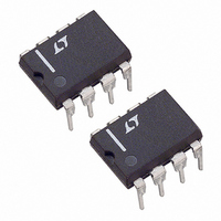
LT1351CN8 Linear Technology, LT1351CN8 Datasheet - Page 10

LT1351CN8
Manufacturer Part Number
LT1351CN8
Description
IC OP-AMP HI-SPEED 3MHZ 8-DIP
Manufacturer
Linear Technology
Series
C-Load™r
Datasheet
1.LT1351CS8PBF.pdf
(16 pages)
Specifications of LT1351CN8
Amplifier Type
Voltage Feedback
Number Of Circuits
1
Slew Rate
200 V/µs
Gain Bandwidth Product
3MHz
Current - Input Bias
20nA
Voltage - Input Offset
200µV
Current - Supply
250µA
Current - Output / Channel
13.4mA
Voltage - Supply, Single/dual (±)
±2.5 V ~ 15 V
Operating Temperature
0°C ~ 70°C
Mounting Type
Through Hole
Package / Case
8-DIP (0.300", 7.62mm)
Lead Free Status / RoHS Status
Contains lead / RoHS non-compliant
Output Type
-
-3db Bandwidth
-
Available stocks
Company
Part Number
Manufacturer
Quantity
Price
Company:
Part Number:
LT1351CN8#PBF
Manufacturer:
Vishay/Siliconix
Quantity:
2 000
Part Number:
LT1351CN8#PBF
Manufacturer:
LINEAR/凌特
Quantity:
20 000
APPLICATIONS
LT1351
noise gain is one and a large feedback resistor is used, C
should be greater than or equal to C
be an I-to-V converter as shown in the Typical Applications
section.
Capacitive Loading
The LT1351 is stable with any capacitive load. As the
capacitive load increases, both the bandwidth and phase
margin decrease so there will be peaking in the frequency
domain and in the transient response. Graphs of Fre-
quency Response vs Capacitive Load, Capacitive Load
Handling and the transient response photos clearly show
these effects.
Input Considerations
Each of the LT1351 inputs is the base of an NPN and
a PNP transistor whose base currents are of opposite
polarity and provide first-order bias current cancellation.
Because of variation in the matching of NPN and PNP
beta, the polarity of the input bias current can be positive
or negative. The offset current does not depend on
NPN/PNP beta matching and is well controlled. The use of
balanced source resistance at each input is recommended
for applications where DC accuracy must be maximized.
The inputs can withstand transient differential input volt-
ages up to 10V without damage and need no clamping or
source resistance for protection. Differential inputs, how-
ever, generate large supply currents (tens of mA) as
required for high slew rates. If the device is used with
sustained differential inputs, the average supply current
will increase, excessive power dissipation will result and
the part may be damaged. The part should not be used as
a comparator, peak detector or other open-loop applica-
tion with large, sustained differential inputs . Under
normal, closed-loop operation, an increase of power
dissipation is only noticeable in applications with large
slewing outputs and is proportional to the magnitude of
the differential input voltage and the percent of the time
that the inputs are apart. Measure the average supply
current for the application in order to calculate the power
dissipation.
10
U
INFORMATION
U
W
IN
. An example would
U
F
Shutdown
The LT1351 has a Shutdown pin for conserving power.
When this pin is open or 2V above the negative supply the
part operates normally. When pulled down to V
supply current will drop to about 10 A. The current out of
the Shutdown pin is also typically 10 A. In shutdown the
amplifier output is not isolated from the inputs so the
LT1351 cannot be used in multiplexing applications using
the shutdown feature.
A level shift application is shown in the Typical Applica-
tions section so that a ground-referenced logic signal can
control the Shutdown pin.
Circuit Operation
The LT1351 circuit topology is a true voltage feedback
amplifier that has the slewing behavior of a current
feedback amplifier. The operation of the circuit can be
understood by referring to the simplified schematic.
The inputs are buffered by complementary NPN and PNP
emitter followers which drive R1, a 1k resistor. The input
voltage appears across the resistor generating currents
which are mirrored into the high impedance node and
compensation capacitor C
form an output stage which buffers the gain node from
the load. The output devices Q19 and Q22 are connected
to form a composite PNP and composite NPN.
The bandwidth is set by the input resistor and the
capacitance on the high impedance node. The slew rate
is determined by the current available to charge the
capacitance. This current is the differential input voltage
divided by R1, so the slew rate is proportional to the
input. Highest slew rates are therefore seen in the lowest
gain configurations. For example, a 10V output step in a
gain of 10 has only a 1V input step whereas the same
output step in unity gain has a 10 times greater input step.
The curve of Slew Rate vs Input Level illustrates this
relationship.
Capacitive load compensation is provided by the R
network which is bootstrapped across the output stage.
When the amplifier is driving a light load the network has
no effect. When driving a capacitive load (or a low value
T
. Complementary followers
–
C
, C
the
C


