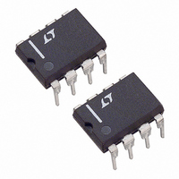
LT1224CN8 Linear Technology, LT1224CN8 Datasheet - Page 6

LT1224CN8
Manufacturer Part Number
LT1224CN8
Description
IC OP-AMP HI-SPEED 45MHZ 8-DIP
Manufacturer
Linear Technology
Datasheet
1.LT1224CS8PBF.pdf
(8 pages)
Specifications of LT1224CN8
Amplifier Type
General Purpose
Number Of Circuits
1
Slew Rate
400 V/µs
Gain Bandwidth Product
45MHz
Current - Input Bias
4µA
Voltage - Input Offset
500µV
Current - Supply
7mA
Current - Output / Channel
40mA
Voltage - Supply, Single/dual (±)
±2.5 V ~ 15 V
Operating Temperature
0°C ~ 70°C
Mounting Type
Through Hole
Package / Case
8-DIP (0.300", 7.62mm)
Lead Free Status / RoHS Status
Contains lead / RoHS non-compliant
Output Type
-
-3db Bandwidth
-
Available stocks
Company
Part Number
Manufacturer
Quantity
Price
Company:
Part Number:
LT1224CN8
Manufacturer:
LT
Quantity:
5 510
Company:
Part Number:
LT1224CN8
Manufacturer:
LT
Quantity:
5 510
Part Number:
LT1224CN8
Manufacturer:
LT/凌特
Quantity:
20 000
Company:
Part Number:
LT1224CN8 ES
Manufacturer:
LT
Quantity:
57
Part Number:
LT1224CN8#PBF
Manufacturer:
LINEAR/凌特
Quantity:
20 000
The LT1224 may be inserted directly into HA2541, HA2544,
AD847, EL2020 and LM6361 applications, provided that
the nulling circuitry is removed. The suggested nulling
circuit for the LT1224 is shown below.
Layout and Passive Components
As with any high speed operational amplifier, care must be
taken in board layout in order to obtain maximum perfor-
mance. Key layout issues include: use of a ground plane,
minimization of stray capacitance at the input pins, short
lead lengths, RF-quality bypass capacitors located close
to the device (typically 0.01 F to 0.1 F), and use of low
ESR bypass capacitors for high drive current applications
(typically 1 F to 10 F tantalum). Sockets should be
avoided when maximum frequency performance is
required, although low profile sockets can provide
reasonable performance up to 50MHz. For more details
see Design Note 50. Feedback resistor values greater than
5k are not recommended because a pole is formed with the
input capacitance which can cause peaking. If feedback
resistors greater than 5k are used, a parallel
capacitor of 5pF to 10pF should be used to cancel the input
pole and optimize dynamic performance.
Transient Response
The LT1224 gain bandwidth is 45MHz when measured at
f = 1MHz. The actual frequency response in unity-gain is
considerably higher than 45MHz due to peaking caused by
a second pole beyond the unity-gain crossover. This is
reflected in the 50 phase margin and shows up as
LT1224
A
6
PPLICATI
O
3
2
U
+
–
LT1224
S
1
Offset Nulling
8
5k
I FOR ATIO
U
V
V
+
–
7
4
6
LT1224 • TA03
W
0.1 F
0.1 F
U
overshoot in the unity-gain small-signal transient re-
sponse. Higher noise gain configurations exhibit less
overshoot as seen in the inverting gain of one response.
The large-signal responses in both inverting and non-
inverting gain show symmetrical slewing characteristics.
Normally the noninverting response has a much faster
rising edge than falling edge due to the rapid change in
input common-mode voltage which affects the tail current
of the input differential pair. Slew enhancement circuitry
has been added to the LT1224 so that the noninverting
slew rate response is balanced.
Input Considerations
Resistors in series with the inputs are recommended for
the LT1224 in applications where the differential input
voltage exceeds 6V continuously or on a transient basis.
An example would be in noninverting configurations with
high input slew rates or when driving heavy capacitive
loads. The use of balanced source resistance at each input
is recommended for applications where DC accuracy must
be maximized.
Small Signal, A
Large Signal, A
V
V
= 1
= 1
Small Signal, A
Large Signal, A
V
V
= –1
= –1
LT1224 • TA04
LT1224 • TA06


