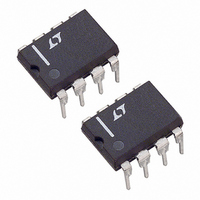
LT1226CN8#PBF Linear Technology, LT1226CN8#PBF Datasheet - Page 3

LT1226CN8#PBF
Manufacturer Part Number
LT1226CN8#PBF
Description
IC OP-AMP HI-SPD LOW NOISE 8-DIP
Manufacturer
Linear Technology
Datasheet
1.LT1226CS8PBF.pdf
(8 pages)
Specifications of LT1226CN8#PBF
Amplifier Type
General Purpose
Number Of Circuits
1
Slew Rate
400 V/µs
Gain Bandwidth Product
1GHz
Current - Input Bias
4µA
Voltage - Input Offset
300µV
Current - Supply
7mA
Current - Output / Channel
40mA
Voltage - Supply, Single/dual (±)
±2.5 V ~ 15 V
Operating Temperature
0°C ~ 70°C
Mounting Type
Through Hole
Package / Case
8-DIP (0.300", 7.62mm)
Lead Free Status / RoHS Status
Lead free / RoHS Compliant
Output Type
-
-3db Bandwidth
-
Available stocks
Company
Part Number
Manufacturer
Quantity
Price
SYMBOL
V
I
I
CMRR
A
V
I
SR
GBW
t
t
I
SYMBOL
V
I
I
CMRR
PSRR
A
V
I
SR
I
Note 1: A heat sink may be required to keep the junction temperature
below absolute maximum when the output is shorted indefinitely.
Note 2: Input offset voltage is tested with automated test equipment
in <1 second.
ELECTRICAL C
ELECTRICAL C
OS
B
OUT
r
s
S
OS
B
OUT
S
OS
VOL
OUT
, t
OS
VOL
OUT
f
PARAMETER
Input Offset Voltage
Input V
Input Offset Current
Input Bias Current
Common-Mode Rejection Ratio
Power Supply Rejection Ratio
Large Signal Voltage Gain
Output Swing
Output Current
Slew Rate
Supply Current
PARAMETER
Input Offset Voltage
Input Offset Current
Input Bias Current
Input Voltage Range +
Input Voltage Range –
Common-Mode Rejection Ratio
Large Signal Voltage Gain
Output Voltage
Output Current
Slew Rate
Full Power Bandwidth
Gain Bandwidth
Rise Time, Fall Time
Overshoot
Propagation Delay
Settling Time
Supply Current
OS
Drift
HARA TERISTICS
HARA TERISTICS
C
C
CONDITIONS
V
V
V
V
V
V
V
V
V
V
V
V
V
V
S
S
S
S
S
S
S
S
S
S
S
S
S
S
= 15V, (Note 2)
=
= 15V and V
= 15V and V
= 15V, V
= 5V to 15V
= 15V, V
= 5V, V
= 15V, R
= 5V, R
= 15V, V
= 5V, V
= 15V, (Note 3)
= 15V and V
5V, (Note 2)
CONDITIONS
(Note 2)
V
V
V
R
R
V
(Note 3)
3V Peak, (Note 4)
f = 1MHz
A
A
50% V
– 2.5V to 2.5V, 0.1%, A
CM
OUT
OUT
OUT
VCL
VCL
OUT
OUT
L
L
L
CM
OUT
OUT
L
V
0 C T
= 500
= 150
= 500 or 150
S
= 500
= 2.5V
= +25, 10% to 90%, 0.1V
= +25, 0.1V
= 2.5V, R
= 2.5V, R
= 3V
= 2.5V, R
= 3V
= 12V and V
= 5V, T
= 10V, R
= 12V
IN
S
S
S
= 5V
= 5V
= 5V
to 50% V
A
70 C, V
A
Note 3: Slew rate is measured between 10V on an output swing of 12V
on 15V supplies, and 2V on an output swing of 3.5V on 5V supplies.
Note 4: Full power bandwidth is calculated from the slew rate
measurement: FPBW = SR/2 Vp.
L
L
L
L
= 25 C, V
= 500
= 150
= 500
OUT
= 500
S
= 5V, V
V
CM
= – 24
= 0V unless otherwise noted.
CM
CM
= 0V unless otherwise noted.
= 2.5V
MIN
2.5
94
50
3.0
3.0
20
MIN
92
92
35
35
12.0
3.0
24
20
250
–3
TYP
1.0
100
4
4
103
100
75
3.7
3.3
40
250
13.3
700
8
25
8
60
7
TYP
0.3
1.0
6
100
4
103
110
150
100
13.3
3.3
40
40
400
7
–2.5
MAX
1.4
400
8
9
MAX
1.3
1.8
600
9
10.5
LT1226
UNITS
UNITS
V/mV
V/mV
V/mV
V/mV
3
V/ s
V/ s
MHz
MHz
V/ C
mV
mA
mA
mV
mV
mA
mA
mA
nA
dB
nA
dB
dB
ns
ns
ns
%
A
V
V
V
V
A
V
V


