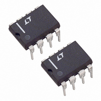
LT1225CN8#PBF Linear Technology, LT1225CN8#PBF Datasheet - Page 7

LT1225CN8#PBF
Manufacturer Part Number
LT1225CN8#PBF
Description
IC OP-AMP HI-SPEED 150MHZ 8-DIP
Manufacturer
Linear Technology
Datasheet
1.LT1225CN8.pdf
(8 pages)
Specifications of LT1225CN8#PBF
Amplifier Type
General Purpose
Number Of Circuits
1
Slew Rate
400 V/µs
Gain Bandwidth Product
150MHz
Current - Input Bias
4µA
Voltage - Input Offset
500µV
Current - Supply
7mA
Current - Output / Channel
40mA
Voltage - Supply, Single/dual (±)
±2.5 V ~ 15 V
Operating Temperature
0°C ~ 70°C
Mounting Type
Through Hole
Package / Case
8-DIP (0.300", 7.62mm)
Lead Free Status / RoHS Status
Lead free / RoHS Compliant
Output Type
-
-3db Bandwidth
-
Available stocks
Company
Part Number
Manufacturer
Quantity
Price
domain and in the transient response. The photo of the
small-signal response with 1000pF load shows 50% peak-
ing. The large-signal response with a 10,000pF load shows
the output slew rate being limited by the short-circuit
current.
A
The LT1225 can drive coaxial cable directly, but for best
pulse fidelity the cable should be doubly terminated with
a resistor in series with the output.
TYPICAL
PPLICATI
A
V
= – 5, C
V
IN
L
A
= 1000pF
500
O
PPLICATI
LAMP
100pF
100pF
#327
1.5k
Wein Bridge Oscillator
U
Lag Compensation
S
A
V
= 1, f < 3MHz
I FOR ATIO
–
+
U
+
–
100pF
LT1225
LT1225
Information furnished by Linear Technology Corporation is believed to be accurate and reliable.
However, no responsibility is assumed for its use. Linear Technology Corporation makes no represen-
tation that the interconnection of circuits as described herein will not infringe on existing patent rights.
430
O
2k
A
1.5k
U
V
= 5, C
W
S
L
= 10,000pF
LT1225 TA03
LT1225 TA05
V
>10V
1MHz
V
OUT
OUT
P-P
U
LT1225 AI04
Compensation
The LT1225 has a typical gain-bandwidth product of
150MHz which allows it to have wide bandwidth in high
gain configurations (i.e., in a gain of 10 it will have a
bandwidth of about 15MHz). The amplifier is stable in a
noise gain of 5 so the ratio of the output signal to the
inverting input must be 1/5 or less. Straightforward gain
configurations of 5 or –4 are stable, but there are a few
configurations that allow the amplifier to be stable for
lower signal gains (the noise gain, however, remains 5 or
more). One example is the summing amplifier shown in
the typical applications section below. Each input signal
has a gain of –R
this configuration is equivalent to a gain of –4 as far as the
amplifier is concerned. Lag compensation can also be
used to give a low frequency gain less than 5 with a high
frequency gain of 5 or greater. The example below has a
DC gain of one, but an AC gain of 5. The break frequency
of the RC combination across the amplifier inputs should
be approximately a factor of 10 less than the gain band-
width of the amplifier divided by the high frequency gain
(in this case 1/10 of 150MHz/5 or 3MHz).
V
IN
V
V
V
R2
250
IN1
IN2
IN
n
+
–
R
LT1225
IN
R
R
R
=
F
IN
IN
IN
/R
nR
1k
R1
4
F
IN
Summing Amplifier
to the output, but it is easily seen that
Cable Driving
–
+
75
LT1225
R3
R
F
75 CABLE
LT1225 TA06
R4
75
V
LT1225 TA04
LT1225
OUT
V
OUT
7


