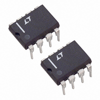
LT1219LCN8#PBF Linear Technology, LT1219LCN8#PBF Datasheet - Page 11

LT1219LCN8#PBF
Manufacturer Part Number
LT1219LCN8#PBF
Description
IC PREC OP-AMP R-R IN/OUT 8-DIP
Manufacturer
Linear Technology
Series
C-Load™r
Datasheet
1.LT1218LCS8PBF.pdf
(16 pages)
Specifications of LT1219LCN8#PBF
Amplifier Type
General Purpose
Number Of Circuits
1
Output Type
Rail-to-Rail
Slew Rate
0.05 V/µs
Gain Bandwidth Product
150kHz
Current - Input Bias
30nA
Voltage - Input Offset
35µV
Current - Supply
400µA
Current - Output / Channel
12mA
Voltage - Supply, Single/dual (±)
2 V ~ 10 V, ±1 V ~ 5 V
Operating Temperature
0°C ~ 70°C
Mounting Type
Through Hole
Package / Case
8-DIP (0.300", 7.62mm)
Lead Free Status / RoHS Status
Lead free / RoHS Compliant
-3db Bandwidth
-
Available stocks
Company
Part Number
Manufacturer
Quantity
Price
TYPICAL PERFORMANCE CHARACTERISTICS
Rail-to-Rail Operation
The LT1218/LT1219 differ from conventional op amps in
the design of both the input and output stages. Figure 1
shows a simplified schematic of the amplifier. The input
stage consists of two differential amplifiers, a PNP stage
APPLICATIONS
V
0.001
+
0.01
0.1
10
1
0
– 300mV
THD + Noise vs
Peak-to-Peak Voltage
SHDN
f = 1kHz
R
(ALL CURVES)
L
= 10k
IN
IN
V
V
INPUT VOLTAGE (PEAK-TO-PEAK)
+
CONTROL
+
–
–
1
Q12
BIAS
V
A
S
V
= 1.5V
= –1
2
Q6
U
Q3 Q4
V
A
3
S
V
= 1.5V
= 1
V
A
INFORMATION
S
V
U
V
A
= 2.5V
= 1
W
S
V
LT1218/19 • TPC26
V
4
= 2.5V
= –1
–
D1
Q5
U
5
D3
Q1 Q2
W
I1
Figure 1. LT1218 Simplified Schematic Diagram
D2
A
V
Small-Signal Response
V
U
Q7
V
S
S
V
= 1
= 15V
+
= 15V
Q10
Q8
TRIM
Q9
Q11
Q13
Q1/Q2 and an NPN stage Q3/Q4, which are active over
different portions of the input common mode range.
Lateral devices are used in both input stages, eliminating
the need for clamps across the input pins. Each input stage
is trimmed for offset voltage. A complementary output
configuration (Q23 through Q26) is employed to create an
V
–
C
C
Q14
D7
D4
Q15
LT1218/18 • TPC27
D5
V
+
Q18
Q16
A
V
Large-Signal Response
V
V
S
S
= 1
= 15V
= 15V
LT1218/LT1219
Q17
Q19
Q20
D6
V
V
Q21
Q22
+
–
C1
C2
V
V
Q23
Q25
–
+
LT1218/19 • F01
D7
D8
11
LT1218/18 • TPC28
Q24
Q26
OUT


