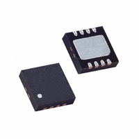
LT6203CDD#TR Linear Technology, LT6203CDD#TR Datasheet - Page 16

LT6203CDD#TR
Manufacturer Part Number
LT6203CDD#TR
Description
IC OP AMP DUAL 100MHZ 3MA 8-DFN
Manufacturer
Linear Technology
Datasheet
1.LT6202CS8PBF.pdf
(24 pages)
Specifications of LT6203CDD#TR
Amplifier Type
General Purpose
Number Of Circuits
2
Output Type
Rail-to-Rail
Slew Rate
25 V/µs
Gain Bandwidth Product
100MHz
Current - Input Bias
3.8µA
Voltage - Input Offset
2600µV
Current - Supply
2.8mA
Current - Output / Channel
40mA
Voltage - Supply, Single/dual (±)
2.5 V ~ 12.6 V, ±1.25 V ~ 6.3 V
Operating Temperature
0°C ~ 70°C
Mounting Type
Surface Mount
Package / Case
8-DFN
Lead Free Status / RoHS Status
Contains lead / RoHS non-compliant
-3db Bandwidth
-
Available stocks
Company
Part Number
Manufacturer
Quantity
Price
LT6202/LT6203/LT6204
APPLICATIONS INFORMATION
Input Protection
There are back-to-back diodes, D1 and D2, across the
+ and – inputs of these amplifi ers to limit the differential
input voltage to ±0.7V. The inputs of the LT6202/LT6203/
LT6304 do not have internal resistors in series with the input
transistors. This technique is often used to protect the input
devices from over voltage that causes excessive currents
to fl ow. The addition of these resistors would signifi cantly
degrade the low noise voltage of these amplifi ers. For
instance, a 100Ω resistor in series with each input would
generate 1.8nV/√Hz of noise, and the total amplifi er noise
voltage would rise from 1.9nV/√Hz to 2.6nV/√Hz. Once
the input differential voltage exceeds ±0.7V, steady state
current conducted though the protection diodes should be
limited to ±40mA. This implies 25Ω of protection resistance
per volt of continuous overdrive beyond ±0.7V. The input
diodes are rugged enough to handle transient currents
due to amplifi er slew rate overdrive or momentary clipping
without these resistors.
Figure 2 shows the input and output waveforms of the
amplifi er driven into clipping while connected in a gain
of A
the power supply rails, the input transistors will saturate.
When saturation occurs, the amplifi er loses a stage of
phase inversion and the output tries to change states.
Diodes D1 and D2 forward bias and hold the output within
16
V
OV
= 1. When the input signal goes suffi ciently beyond
Figure 2. V
S
= ±2.5V, A
V
= 1 with Large Overdrive
a diode drop of the input signal. In this photo, the input
signal generator is clipping at ±35mA, and the output
transistors supply this generator current through the
protection diodes.
With the amplifi er connected in a gain of A
can invert with very heavy input overdrive. To avoid this
inversion, limit the input overdrive to 0.5V beyond the
power supply rails.
ESD
The LT6202/LT6203/LT6204 have reverse-biased ESD
protection diodes on all inputs and outputs as shown in
Figure 1. If these pins are forced beyond either supply,
unlimited current will fl ow through these diodes. If the
current is transient and limited to one hundred milliamps
or less, no damage to the device will occur.
Noise
The noise voltage of the LT6202/LT6203/LT6204 is equiva-
lent to that of a 225Ω resistor, and for the lowest possible
noise it is desirable to keep the source and feedback
resistance at or below this value, i.e. R
With R
is: e
tance value, the amplifi er dominates the noise, but in the
resistance region between 225Ω and approximately 10kΩ,
the noise is dominated by the resistor thermal noise. As
the total resistance is further increased, beyond 10k, the
noise current multiplied by the total resistance eventually
dominates the noise.
The product of e
low noise amplifi ers. Many low noise amplifi ers with low e
have high I
noise with the lowest possible supply current, this product
can prove to be enlightening. The LT6202/LT6203/LT6204
have an e
common to see amplifi ers with similar noise specifi cations
have an e
For a complete discussion of amplifi er noise, see the
LT1028 data sheet.
n
= √(1.9nV)
S
+ R
n
n
, √I
SUPPLY
• √I
G
||
SUPPLY
R
SUPPLY
FB
n
• √I
2
current. In applications that require low
= 225Ω the total noise of the amplifi er
+(1.9nV)
SUPPLY
product of 3.2 per amplifi er, yet it is
product of 4.7 to 13.5.
2
is an interesting way to gauge
= 2.7nV. Below this resis-
S
+ R
V
G
≥ 2, the output
||
R
FB
≤ 225Ω.
620234fb
n


