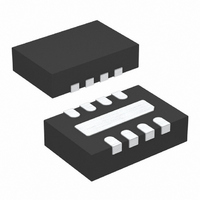
LT6203CDD#TRPBF Linear Technology, LT6203CDD#TRPBF Datasheet - Page 9

LT6203CDD#TRPBF
Manufacturer Part Number
LT6203CDD#TRPBF
Description
IC OPAMP R-R IN/OUT DUAL LP 8DFN
Manufacturer
Linear Technology
Datasheet
1.LT6202CS8PBF.pdf
(24 pages)
Specifications of LT6203CDD#TRPBF
Amplifier Type
General Purpose
Number Of Circuits
2
Output Type
Rail-to-Rail
Slew Rate
25 V/µs
Gain Bandwidth Product
100MHz
Current - Input Bias
3.8µA
Voltage - Input Offset
2600µV
Current - Supply
2.8mA
Current - Output / Channel
40mA
Voltage - Supply, Single/dual (±)
2.5 V ~ 12.6 V, ±1.25 V ~ 6.3 V
Operating Temperature
0°C ~ 70°C
Mounting Type
Surface Mount
Package / Case
8-DFN
Lead Free Status / RoHS Status
Lead free / RoHS Compliant
-3db Bandwidth
-
Available stocks
Company
Part Number
Manufacturer
Quantity
Price
ELECTRICAL CHARACTERISTICS
temperature range. V
SYMBOL PARAMETER
V
I
ΔI
I
A
CMRR
PSRR
V
V
I
I
GBW
SR
FPBW
Note 1: Stresses beyond those listed under Absolute Maximum Ratings
may cause permanent damage to the device. Exposure to any Absolute
Maximum Rating condition for extended periods may affect device
reliability and lifetime.
Note 2: Inputs are protected by back-to-back diodes and diodes to each
supply. If the inputs are taken beyond the supplies or the differential input
voltage exceeds 0.7V, the input current must be limited to less than 40mA.
Note 3: A heat sink may be required to keep the junction temperature
below the absolute maximum rating when the output is shorted
indefi nitely.
Note 4: The LT6202C/LT6202I, LT6203C/LT6203I and LT6204C/LT6204I are
guaranteed functional over the temperature range of –40°C and 85°C.
Note 5: The LT6202C/LT6203C/LT6204C are guaranteed to meet specifi ed
performance from 0°C to 70°C. The LT6202C/LT6203C/LT6204C are
designed, characterized and expected to meet specifi ed performance from
–40°C to 85°C, but are not tested or QA sampled at these temperatures.
The LT6202I/LT6203I/LT6204I are guaranteed to meet specifi ed
performance from –40°C to 85°C.
B
OS
SC
S
VOL
OS
OL
OH
B
TC
Input Offset Voltage Drift (Note 9)
Input Offset Voltage Match
(Channel-to-Channel) (Note 6)
Input Bias Current
I
I
Input Offset Current
Large Signal Gain
Common Mode Rejection Ratio
CMRR Match (Channel-to-Channel) (Note 6)
Power Supply Rejection Ratio
PSRR Match (Channel-to-Channel) (Note 6)
Output Voltage Swing LOW Saturation
(Note 8)
Output Voltage Swing HIGH Saturation
(Note 8)
Short-Circuit Current
Supply Current per Amp
Gain Bandwidth Product
Slew Rate
Full Power Bandwidth (Note 10)
B
B
Shift
Match (Channel-to-Channel) (Note 6)
S
= ±5V; V
CM
= V
OUT
= 0V, unless otherwise noted. (Note 5)
CONDITIONS
V
V
V
V
V
V
V
V
V
V
V
V
V
V
V
V
V
No Load
I
I
No Load
I
I
Frequency = 1MHz
A
V
SINK
SINK
SOURCE
SOURCE
CM
CM
CM
CM
CM
CM
CM
CM
CM
CM
O
O
CM
CM
CM
S
S
V
OUT
= ±1.5V to ±5V
= ±1.5V to ±5V
= –1, R
= ±4.5V, R
= ±1.5V R
The
= Half Supply
= 0V
= V
= Half Supply
= V
= V
= V
= Half Supply
= V
= V
= V
= –2V to 2V
= –2V to 2V
= 5mA
= 15mA
= 3V
+
–
–
+
–
–
–
= 5mA
= 15mA
l
to V
to V
to V
P-P
L
denotes the specifi cations which apply over –40°C < T
= 1k, V
L
+
+
+
L
= 1k
= 100
Note 6: Matching parameters are the difference between the two amplifi ers
A and D and between B and C of the LT6204; between the two amplifi ers
of the LT6203. CMRR and PSRR match are defi ned as follows: CMRR and
PSRR are measured in μV/V on the identical amplifi ers. The difference is
calculated between the matching sides in μV/V. The result is converted to dB.
Note 7: Minimum supply voltage is guaranteed by power supply rejection
ratio test.
Note 8: Output voltage swings are measured between the output and
power supply rails.
Note 9: This parameter is not 100% tested.
Note 10: Full-power bandwidth is calculated from the slew rate:
FPBW = SR/2πV
Note 11: Differential gain and phase are measured using a Tektronix
TSG120YC/NTSC signal generator and a Tektronix 1780R Video
Measurement Set. The resolution of this equipment is 0.1% and 0.1°. Ten
identical amplifi er stages were cascaded giving an effective resolution of
0.01% and 0.01°.
O
= 4V
LT6202/LT6203/LT6204
P
l
l
l
l
l
l
l
l
l
l
l
l
l
l
l
l
l
l
l
l
l
l
l
l
l
l
l
l
l
–7.0
MIN
–10
±15
6.0
1.4
60
65
80
80
60
70
13
–1.4
–4.5
0.15
0.15
TYP
110
110
100
260
130
360
±25
7.5
0.3
0.6
1.8
5.4
0.3
0.5
3.8
1.9
13
84
95
70
98
70
90
18
7
A
MAX
205
500
130
250
640
1.0
2.5
3.6
0.7
1.2
1.6
4.5
< 85°C
24
13
75
1
620234fb
UNITS
μV/°C
V/mV
V/mV
9
MHz
MHz
V/μs
mV
mV
mV
mV
mV
mV
mV
mV
mA
mA
μA
μA
μA
μA
μA
μA
μA
μA
dB
dB
dB
dB
dB


