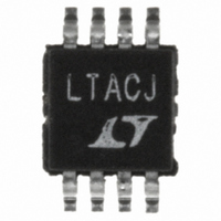
LTC1992-1CMS8#TRPBF Linear Technology, LTC1992-1CMS8#TRPBF Datasheet - Page 28

LTC1992-1CMS8#TRPBF
Manufacturer Part Number
LTC1992-1CMS8#TRPBF
Description
IC AMP/DVR I/O GAIN-1 DIFF 8MSOP
Manufacturer
Linear Technology
Datasheet
1.LTC1992CMS8PBF.pdf
(42 pages)
Specifications of LTC1992-1CMS8#TRPBF
Amplifier Type
Differential
Number Of Circuits
1
Output Type
Differential, Rail-to-Rail
Slew Rate
1.5 V/µs
Gain Bandwidth Product
3.2MHz
Current - Input Bias
2pA
Voltage - Input Offset
250µV
Current - Supply
700µA
Current - Output / Channel
30mA
Voltage - Supply, Single/dual (±)
2.7 V ~ 11 V, ±1.35 V ~ 5.5 V
Operating Temperature
0°C ~ 70°C
Mounting Type
Surface Mount
Package / Case
8-MSOP, Micro8™, 8-uMAX, 8-uSOP,
Lead Free Status / RoHS Status
Lead free / RoHS Compliant
-3db Bandwidth
-
Available stocks
Company
Part Number
Manufacturer
Quantity
Price
LTC1992 Family
applicaTions inForMaTion
Single-Ended to Differential Conversion
One of the most important applications of fully differential
amplifiers is single-ended signaling to differential signaling
conversion. Many systems have a single-ended signal that
must connect to an ADC with a differential input. The ADC
could be run in a single-ended manner, but performance
usually degrades. Fortunately, all of basic applications
circuits shown in Figure 4, as well as all of the fixed gain
LTC1992-X parts, are equally suitable for both differential
and single-ended input signals. For single-ended input
signals, connect one of the inputs to a reference voltage
(e.g., ground or mid-supply) and connect the other to
the signal path. There are no tradeoffs here as the part’s
performance is the same with single-ended or differential
Figure 3. Fully Differential Amplifier Signal Conventions (Ideal Amplifier and Perfect Resistor Matching is Assumed)
4AV
V
P-PDIFF
INDIFF
DIFFERENTIAL
INPUT VOLTAGE
INPUT COMMON
MODE VOLTAGE
+V
–V
V
V
V
V
CMRR =
OUTPUT BALANCE =
e
V
V
A
NOUT
OUTDIFF
AMPDIFF
AMPCM
OUTCM
OSDIFFOUT
OSCM
OUT
OUT
–A
A
–A
=
=
=
= V
= V
( )
=
(
(
= V
∆V
R
= V
∆V
R
+V
–V
OUTCM
V
FB
IN
OCM
AMPDIFF
= V
AMPCM
2AV
2AV
IN
IN
INDIFF
INP
V
INP
+ 1
INCM
OSDIFFIN
– –V
– +V
+ V
P-P
P-P
– V
2
= V
– V
= V
•
•
INM
IN
IN
√
INM
INDIFF
R
R
; +V
OCM
INCM
–V
+V
e
)
)
FB
IN
∆V
∆V
NIN
•
•
IN
IN
•
IN
OUTDIFF
OUTCM
1
2
1
2
( )
2
= +V
=
R
R
= –V
+ r
•
•
FB
IN
+V
R
R
R
R
N
R
R
IN
IN
+ 1
FB
IN
FB
IN
2
IN
IN
IN
– –V
+ –V
2
WHERE: e
+ V
+ V
V
OCM
IN
IN
OCM
OCM
e
r
(RESISTIVE NOISE IS ALREADY INCLUDED IN THE
SPECIFICATIONS FOR THE FIXED GAIN LTC1992-X PARTS)
INM
N
NOUT
NIN
INP
; V
; V
≈ (0.13nV/√Hz)
OSCM
OSCM
= INPUT REFERRED NOISE VOLTAGE DENSITY
DIFFERENTIAL
OUTPUT VOLTAGE
OUTPUT COMMON
MODE VOLTAGE
V
= OUTPUT REFERRED NOISE VOLTAGE DENSITY
–
+
OCM
R
R
= 0V
= 0V
input signals. Which input is used for the signal path only
affects the polarity of the differential output signal.
Signal Level Shifting
Another important application of fully differential ampli-
fier is signal level shifting. Single-ended to differential
conversion accompanied by a signal level shift is very
commonplace when driving ADCs. As noted in the theory of
operation section, fully differential amplifiers have a com-
mon mode level servo that determines the output common
mode level independent of the input common mode level.
To set the output common mode level, simply apply the
desired voltage to the V
on the V
FB
FB
+
–
LTC1992
(
R
R
IN
IN
+ R
• R
1992 F03
OCM
= V
= V
FB
FB
)
OUTDIFF
OUTCM
V
OUTCM
+V
–V
pin is from (–V
OUT
OUT
=
= +V
+V
–B
OUT
OUT
B
+ –V
2
–B
B
– –V
OUT
OUT
2BV
2BV
OCM
P-P
P-P
S
input pin. The voltage range
V
4BV
OUTDIFF
+ 0.5V) to (+V
P-PDIFF
S
– 1.3V).
1992fa


