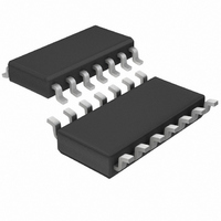
LT1882IS Linear Technology, LT1882IS Datasheet

LT1882IS
Specifications of LT1882IS
Available stocks
Related parts for LT1882IS
LT1882IS Summary of contents
Page 1
... Instrumentation Amplifi ers n Battery-Powered Systems n Photo Current Amplifi ers L, LT, LTC, LTM, Linear Technology and the Linear logo are registered trademarks of Linear Technology Corporation. All other trademarks are the property of their respective owners. TYPICAL APPLICATION 16-Bit Voltage Output DAC on ± 5V Supply ...
Page 2
... Plastic SO 1881I 8-Lead Plastic SO LT1881ACN8 8-Lead PDIP LT1881AIN8 8-Lead PDIP 1881A 8-Lead Plastic SO 1881AI 8-Lead Plastic SO LT1882CS 14-Lead Plastic SO LT1882IS 14-Lead Plastic SO LT1882HS 14-Lead Plastic SO LT1882MPS 14-Lead Plastic SO http://www.linear.com/leadfree/ http://www.linear.com/tapeandreel/ TOP VIEW 14 OUT A 1 OUT D 13 – – ...
Page 3
ELECTRICAL CHARACTERISTICS temperature range, otherwise specifi cations are at T (Note 5) SYMBOL PARAMETER V Input Offset Voltage (LT1881A) OS Input Offset Voltage (LT1881/LT1882) ΔV /ΔT Input Offset Voltage Drift OS (Note 6) ΔV Long-Term Input Offset / OS ΔTIME ...
Page 4
LT1881/LT1882 ELECTRICAL CHARACTERISTICS temperature range, otherwise specifi cations are at T (Note 5) SYMBOL PARAMETER A Large-Signal Voltage Gain VOL V Output Voltage Swing Low OL V Output Voltage Swing High OH + (Referred Supply Current ...
Page 5
ELECTRICAL CHARACTERISTICS temperature range, otherwise specifi cations are at T (Note 5) SYMBOL PARAMETER ΔI Noninverting Bias Current Match + B (LT1881/LT1882) ΔCMRR Common Mode Rejection Ratio Match ΔPSRR Power Supply Rejection Match (Notes 7, 9) The l denotes the ...
Page 6
LT1881/LT1882 ELECTRICAL CHARACTERISTICS temperature range, otherwise specifi cations are at T (Note 5) SYMBOL PARAMETER Input Noise Voltage e Input Noise Voltage Density n i Input Noise Current Density n R Input Resistance IN C Input Capacitance IN V Input ...
Page 7
ELECTRICAL CHARACTERISTICS ELECTRICAL CHARACTERISTICS temperature range, otherwise specifi cations are at T (Note 5) SYMBOL PARAMETER FPBW Full-Power Bandwidth ΔV Offset Voltage Match OS (LT1881A) Offset Voltage Match (LT1881/LT1882) Offset Voltage Match Drift ΔI Noninverting Bias Current Match + B ...
Page 8
LT1881/LT1882 TYPICAL PERFORMANCE CHARACTERISTICS Supply Current per Amplifi Supply Voltage 1200 125°C 1000 800 25°C 600 –55°C 400 200 TOTAL SUPPLY VOLTAGE (V) 18812 G01 Settling Time vs ...
Page 9
TYPICAL PERFORMANCE CHARACTERISTICS Gain vs Frequency with ±15V S 0 –10 –20 –30 –40 1k 10k 100k FREQUENCY (Hz) Large Signal Response –1 V 18812 G12 TIME (50μs/DIV) Small Signal ...
Page 10
LT1881/LT1882 TYPICAL PERFORMANCE CHARACTERISTICS V Distribution 25° ±15V LOT) 20 144 S8 (2 LOTS) 18 184 TOTAL PARTS ...
Page 11
TYPICAL PERFORMANCE CHARACTERISTICS Output Saturation Voltage vs Load Current (Output Low ±15V 30mV OVERDRIVE 1 0 –55° –40° 25° 85° ...
Page 12
LT1881/LT1882 TYPICAL PERFORMANCE CHARACTERISTICS Common Mode Rejection Ratio vs Frequency 120 100 0 100 1k 10k 100k 1M FREQUENCY (Hz) 1881/2 G36 Noise Current Density vs Frequency 180 V = ±15V S 160 ...
Page 13
TYPICAL PERFORMANCE CHARACTERISTICS Total Harmonic Distortion + Noise vs Output Voltage Amplitude – ±2. – ±15V S 0 ±2.5V S 0.01 ...
Page 14
LT1881/LT1882 APPLICATIONS INFORMATION The LT1881 dual and LT1882 quad op amps feature exceptional input precision with rail-to-rail output swing. The amplifi ers are similar to the LT1884 and LT1885 devices. The LT1881 and LT1882 offer superior capacitive load driving capabilities ...
Page 15
PACKAGE DESCRIPTION .300 – .325 (7.620 – 8.255) .008 – .015 (0.203 – 0.381) +.035 .325 –.015 ( ) +0.889 8.255 –0.381 NOTE: 1. DIMENSIONS ARE MILLIMETERS *THESE DIMENSIONS DO NOT INCLUDE MOLD FLASH OR PROTRUSIONS. MOLD FLASH OR PROTRUSIONS ...
Page 16
LT1881/LT1882 PACKAGE DESCRIPTION .050 BSC .245 MIN .030 ±.005 TYP RECOMMENDED SOLDER PAD LAYOUT .010 – .020 (0.254 – 0.508) .008 – .010 (0.203 – 0.254) (0.406 – 1.270) NOTE: 1. DIMENSIONS IN (MILLIMETERS) 2. DRAWING NOT TO SCALE 3. ...
Page 17
... MOLD FLASH OR PROTRUSIONS SHALL NOT EXCEED .006" (0.15mm) Information furnished by Linear Technology Corporation is believed to be accurate and reliable. However, no responsibility is assumed for its use. Linear Technology Corporation makes no representation that the interconnection of its circuits as described herein will not infringe on existing patent rights. ...
Page 18
... Lower Power, Available in DFN Package I = 1pA Max www.linear.com ● REF CC 1μF +IN CLK LTC1287 –IN D OUT GND CS/SHDN 18812 TA02 , – 40°C to 85°C Operation Guaranteed, SOT-23 Package OS = 70μV Max OS LT 0809 REV B • PRINTED IN USA © LINEAR TECHNOLOGY CORPORATION 2000 18812fb ...


