LTC1151CSW Linear Technology, LTC1151CSW Datasheet
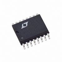
IC OPAMP ZERO-DRIFT DUAL 16SOIC

LTC1151CSW

Manufacturer Part Number
LTC1151CSW
Description
IC OPAMP ZERO-DRIFT DUAL 16SOIC
Manufacturer
Linear Technology
Datasheet

Specifications of LTC1151CSW

Amplifier Type
Chopper (Zero-Drift)
Number Of Circuits
2
Slew Rate
2.5 V/µs
Gain Bandwidth Product
2MHz
Current - Input Bias
15pA
Voltage - Input Offset
0.5µV
Current - Supply
900µA
Voltage - Supply, Single/dual (±)
4.75 V ~ 36 V, ±2.38 V ~ 18 V
Operating Temperature
0°C ~ 70°C
Mounting Type
Surface Mount
Package / Case
16-SOIC (0.300", 7.5mm Width)
Lead Free Status / RoHS Status
Contains lead / RoHS non-compliant
Output Type
-
Current - Output / Channel
-
-3db Bandwidth
-
Other names
LTC1151CS

Available stocks

Company
Part Number
Manufacturer
Quantity
Price
Part Number:
LTC1151CSW
Quantity:
9 000
Part Number:
LTC1151CSW
Manufacturer:
LT
Quantity:
1 000
Part Number:
LTC1151CSW
Manufacturer:
LT
Quantity:
20 000
Part Number:
LTC1151CSW#PBF
Manufacturer:
LTC
Quantity:
200
Part Number:
LTC1151CSW#PBF
Manufacturer:
LT
Quantity:
309
FEATURES
TYPICAL APPLICATIO
APPLICATIO S
Maximum Offset Voltage Drift: 0.05µV/°C
High Voltage Operation: ±18V
No External Components Required
Maximum Offset Voltage: 5µV
Low Noise: 1.5µV
Minimum Voltage Gain: 125dB
Minimum CMRR: 106dB
Minimum PSRR: 110dB
Low Supply Current: 0.9mA/Amplifier
Single Supply Operation: 4.75V to 36V
Input Common Mode Range Includes Ground
Typical Overload Recovery Time: 20ms
Available in 8-Lead N8 and 16-Lead SW Packages
Strain Gauge Amplifiers
Instrumentation Amplifiers
Electronic Scales
Medical Instrumentation
Thermocouple Amplifiers
High Resolution Data Acquisition
* FULL SCALE TRIM: TRIM FOR 10.0V OUTPUT
WITH THERMOCOUPLE AT 100°C
GND
LT1025
4
15V
V
IN
R
V
5
K
O
–15V
3
7
470k
U
±15V Dual Thermocouple Amplifier
P-P
(0.1Hz to 10Hz)
TYPE K
TYPE K
+
+
51Ω 100Ω*
51Ω 100Ω*
U
2k
2k
6
5
2
3
+
+
LTC1151
LTC1151
1/2
1/2
–15V
4
8
0.1µF
0.1µF
240k
240k
7
1
0.1µF
15V
OUTPUT A
100mV/°C
OUTPUT B
100mV/°C
DESCRIPTIO
1151 TA01
The LTC
zero-drift operational amplifier. The two sample-and-hold
capacitors per amplifier required externally by other chop-
per amplifiers are integrated on-chip. The LTC1151 also
incorporates proprietary high voltage CMOS structures
which allow operation at up to 36V total supply voltage.
The LTC1151 has a typical offset voltage of 0.5µV,
drift of 0.01µV/°C, 0.1Hz to 10Hz input noise voltage of
1.5µV
rate of 3V/µs and a gain-bandwidth product of 2.5MHz
with a supply current of 0.9mA per amplifier. Overload
recovery times from positive and negative saturation are
3ms and 20ms, respectively.
The LTC1151 is available in a standard 8-lead plastic DIP
package as well as a 16-lead wide body SO. The LTC1151
is pin compatible with industry-standard dual op amps
and runs from standard ±15V supplies, allowing it to plug
in to most standard bipolar op amp sockets while offering
significant improvement in DC performance.
All other trademarks are the property of their respective owners.
0.1µF
, LTC and LT are registered trademarks of Linear Technology Corporation.
P-P
®
, and a typical voltage gain of 140dB. It has a slew
1151 is a high voltage, high performance dual
Operational Amplifier
60
50
40
30
20
10
Dual ±15V Zero-Drift
0
U
1
Noise Spectrum
10
FREQUENCY (Hz)
100
1k
LTC1151
1151 TA02
10k
1151fa
1

Related parts for LTC1151CSW

LTC1151CSW Summary of contents

Page 1

... DC performance. , LTC and LT are registered trademarks of Linear Technology Corporation. All other trademarks are the property of their respective owners. 240k 15V 0.1µ ...

Page 2

... V to 12V = ±2.375V to ±16V = ±10V = 10k, V OUT ORDER PART TOP VIEW NUMBER LTC1151CSW 13 OUT B 12 – + PACKAGE = 110°C, θ = 200° LTC1151C MIN TYP MAX ±0.5 ±5 ±0.01 ± ...

Page 3

ELECTRICAL C HARA TERISTICS C temperature range, otherwise specifications are at T PARAMETER CONDITIONS Maximum Output Voltage Swing Slew Rate R L Gain-Bandwidth Product Supply Current per Amplifier No Load Load Internal ...

Page 4

LTC1151 W U TYPICAL PERFOR A Supply Current vs Supply Voltage 2 25°C A 2.0 1.5 1.0 0 TOTAL SUPPLY VOLTAGE (V) 1151 G01 Output Short-Circuit Current vs ...

Page 5

W U TYPICAL PERFOR A CE CHARACTERISTICS Input Bias Current Magnitude vs Temperature 1000 ±15V V S 100 10 1 –50 – 125 100 TEMPERATURE (°C) 1151 G10 0.1Hz to 10Hz ...

Page 6

LTC1151 TEST CIRCUITS 100pF 100k – 10Ω LTC1151 –5V 6 Offset Voltage Test Circuit – 6 LTC1151 – V DC-10Hz Noise Test Circuit 5V ...

Page 7

PPLICATI S I FOR ATIO ACHIEVING PICOAMPERE/MICROVOLT PERFORMANCE Picoamperes In order to realize the picoampere level of accuracy of the LTC1151 proper care must be exercised. Leakage currents in circuitry external to the amplifier can significantly ...

Page 8

LTC1151 PPLICATI S I FOR ATIO A Resistors are another source of thermal EMF errors. Table 1 shows the thermal EMF generated for different resistors. The temperature gradient across the resistor is important, not the ambient temperature. ...

Page 9

U O TYPICAL A PPLICATI 1M –IN S High Voltage Instrumentation Amplifier 0.1µ – – LTC1151 3 1/2 + LTC1151 5 + +IN V LTC1151 7 V OUT GAIN = ...

Page 10

LTC1151 PACKAGE DESCRIPTIO .300 – .325 (7.620 – 8.255) .008 – .015 (0.203 – 0.381) +.035 .325 –.015 ( +0.889 8.255 –0.381 NOTE: 1. DIMENSIONS ARE *THESE DIMENSIONS DO NOT INCLUDE MOLD FLASH OR PROTRUSIONS. MOLD FLASH OR PROTRUSIONS SHALL ...

Page 11

PACKAGE DESCRIPTIO .030 ±.005 TYP N .420 MIN RECOMMENDED SOLDER PAD LAYOUT .291 – .299 (7.391 – 7.595) NOTE 4 .010 – .029 × 45° (0.254 – 0.737) .005 (0.127) RAD MIN .009 – .013 NOTE 3 ...

Page 12

... Rail-to-Rail, MS8, 116dB, Two Resistors Set Gain 150µA per Amplifier (Max), SOT-23/MS8 Package www.linear.com ● 49.9k – 1/2 V OUT LTC1151 A = 100 V + 499Ω 1151 TA04 = 2.7V to 44V Precision Op Amp = 400pA 2.7V to 40V S LT 1105 REV A • PRINTED IN USA © LINEAR TECHNOLOGY CORPORATION 1993 1151fa ...

Related keywords