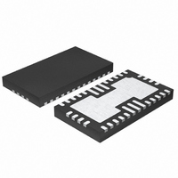
LT6604CUFF-10#PBF Linear Technology, LT6604CUFF-10#PBF Datasheet

LT6604CUFF-10#PBF
Specifications of LT6604CUFF-10#PBF
Available stocks
Related parts for LT6604CUFF-10#PBF
LT6604CUFF-10#PBF Summary of contents
Page 1
... L, LT, LTC and LTM are registered trademarks of Linear Technology Corporation. All other trademarks are the property of their respective owners. 3V ...
Page 2
... MID Lead Temperature (Soldering, 10 sec) .................. 300°C ORDER INFORMATION LEAD FREE FINISH TAPE AND REEL LT6604CUFF-10#PBF LT6604CUFF-10#TRPBF LT6604IUFF-10#PBF LT6604IUFF-10#TRPBF Consult LTC Marketing for parts specifi ed with wider operating temperature ranges. *The temperature grade is identifi label on the shipping container. Consult LTC Marketing for information on non-standard lead based fi nish parts. ...
Page 3
ELECTRICAL CHARACTERISTICS range, otherwise specifi cations are PARAMETER Filter Gain Either Channel Matching of Filter Gain Matching of Filter Phase Filter Gain Either Channel, V ...
Page 4
LT6604-10 ELECTRICAL CHARACTERISTICS range, otherwise specifi cations are PARAMETER Input Bias Current Input Referred Differential Offset Differential Offset Drift Input Common Mode Voltage (Note 3) Output Common Mode Voltage (Note 5) Output Common Mode Offset (with Respect ...
Page 5
TYPICAL PERFORMANCE CHARACTERISTICS Amplitude Response 10 0 –10 –20 –30 –40 –50 –60 –70 –80 100k 1M FREQUENCY (Hz) Passband Gain and Group Delay 12 11 GAIN GROUP DELAY ...
Page 6
LT6604-10 TYPICAL PERFORMANCE CHARACTERISTICS Distortion vs Signal Level 800Ω at Each Output 25°C, Gain = 1 A –40 2ND HARMONIC, 5MHz INPUT 3RD HARMONIC, –50 5MHz INPUT 2ND HARMONIC, –60 1MHz ...
Page 7
PIN FUNCTIONS +INA and –INA (Pins 2, 4): Channel A Input Pins. Signals can be applied to either or both input pins through identi- cal external resistors The DC gain from differential IN inputs to the differential outputs ...
Page 8
LT6604-10 BLOCK DIAGRAM +INA + –INA – OCMA 6 – MIDB +INB IN + ...
Page 9
APPLICATIONS INFORMATION Interfacing to the LT6604-10 Note: The LT6604-10 contains two identical fi lters. The following applications information only refers to one fi lter. The two fi lters are independent except that they share the same negative supply voltage V ...
Page 10
LT6604-10 APPLICATIONS INFORMATION In Figure 3 the LT6604-10 is providing 12dB of gain. The gain resistor has an optional 62pF in parallel to improve the passband fl atness near 10MHz. The common mode output voltage is set to 2V. Use ...
Page 11
APPLICATIONS INFORMATION 2.5V 0.1μF COILCRAFT NETWORK TTWB-1010 ANALYZER 25 388Ω 1:1 SOURCE 4 – 1/2 34 50Ω LT6604-10 53.6Ω 6 – 388Ω 7 0.1μF –2.5V Figure 5 Figure laboratory setup that can ...
Page 12
LT6604-10 APPLICATIONS INFORMATION The LT6604-10 was designed to process a variety of input signals including signals centered on the mid-sup- ply voltage and signals that swing between ground and a positive voltage in a single supply system (Figure 1). The ...
Page 13
APPLICATIONS INFORMATION Figure 8 is plot of the noise spectral density as a function of frequency for an LT6604-10 channel with R using the fi xture of Figure 7 (the instrument noise has been subtracted from the results). The noise ...
Page 14
LT6604-10 TYPICAL APPLICATION Amplitude Response 10 0 –10 –20 –30 –40 –50 –60 DIFFERENTIAL GAIN = 1 – 200Ω 82pF –80 100k 1M 10M FREQUENCY (Hz) 14 Dual, Matched, 5th Order, 10MHz Lowpass Filter + V ...
Page 15
... ON THE TOP AND BOTTOM OF PACKAGE Information furnished by Linear Technology Corporation is believed to be accurate and reliable. However, no responsibility is assumed for its use. Linear Technology Corporation makes no representa- tion that the interconnection of its circuits as described herein will not infringe on existing patent rights. UFF Package 34-Lead Plastic QFN (4mm × ...
Page 16
... SNR = 82dB at 3V Supply, 4 SNR = 76dB at 3V Supply, 4 www.linear.com ● th Order, Differential th Order, Differential th Order Filter th Order Filter th Order Filter th Order Filter th Order Filter th Order Filter th Order Filter th Order Filter 660410fb LT 0409 REV B • PRINTED IN USA © LINEAR TECHNOLOGY CORPORATION 2008 ...


