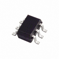
AD8029AKSZ-R2 Analog Devices Inc, AD8029AKSZ-R2 Datasheet - Page 16

AD8029AKSZ-R2
Manufacturer Part Number
AD8029AKSZ-R2
Description
IC AMP GP R-R LP 170MA SC70-6
Manufacturer
Analog Devices Inc
Datasheet
1.AD8029ARZ.pdf
(20 pages)
Specifications of AD8029AKSZ-R2
Slew Rate
63 V/µs
Amplifier Type
General Purpose
Number Of Circuits
1
Output Type
Rail-to-Rail
-3db Bandwidth
125MHz
Current - Input Bias
1.7µA
Voltage - Input Offset
2000µV
Current - Supply
1.4mA
Current - Output / Channel
170mA
Voltage - Supply, Single/dual (±)
2.7 V ~ 12 V, ±1.35 V ~ 6 V
Operating Temperature
-40°C ~ 125°C
Mounting Type
Surface Mount
Package / Case
SC-70-6, SC-88, SOT-363
Op Amp Type
Low Power
No. Of Amplifiers
1
Bandwidth
125MHz
Supply Voltage Range
2.7V To 12V
Amplifier Case Style
SC-70
No. Of Pins
6
Lead Free Status / RoHS Status
Lead free / RoHS Compliant
Gain Bandwidth Product
-
Lead Free Status / RoHS Status
Lead free / RoHS Compliant, Lead free / RoHS Compliant
Other names
AD8029AKSZ-R2TR
Available stocks
Company
Part Number
Manufacturer
Quantity
Price
Part Number:
AD8029AKSZ-R2
Manufacturer:
ADI/亚德诺
Quantity:
20 000
AD8029/AD8030/AD8040
APPLICATIONS
WIDEBAND OPERATION
OUTPUT LOADING SENSITIVITY
To achieve maximum performance and low power dissipation,
the designer needs to consider the loading at the output of
AD8029/AD8030/AD8040. Table 5 shows the effects of output
loading and performance.
When operating at unity gain, the effective load at the amplifier
output is the resistance (R
gains other than 1, in noninverting configurations, the feedback
network represents an additional current load at the amplifier
output. The feedback network (R
which lowers the effective resistance at the output of the
amplifier. The lower effective resistance causes the amplifier to
supply more current at the output. Lower values of feedback
resistance increase the current draw, thus increasing the
amplifier’s power dissipation.
Figure 51. Wideband Non-inverting Gain Configuration
Figure 52. Wideband Inverting Gain Configuration
V
IN
R1 = R
V
IN
R1 = R
R
F
G
R
||R
G
F
||R
R1
G
R1
G
L
–
AD8029
+
) being driven by the amplifier. For
–
AD8029
+
+V
–V
R
+V
–V
S
S
F
R
S
F
S
F
0.1µF
0.1µF
10µF
10µF
C2
C1
C4
C3
0.1µF
0.1µF
+ R
10µF
10µF
C2
C1
C4
C3
G
) is in parallel with R
DISABLE
DISABLE
03679-0-052
03679-0-053
V
OUT
V
OUT
L
Rev. A | Page 16 of 20
,
For example, if using the values shown in Table 5 for a gain of 2,
with resistor values of 2.5 kΩ, the effective load at the output is
1.67 kΩ. For inverting configurations, only the feedback resistor
R
that specified in the data sheet, the amplifier can introduce
nonlinearities in its open-loop response, which increases
distortion. Figure 53 and Figure 54 illustrate effective output
loading and distortion performance. Increasing the resistance of
the feedback network can reduce the current consumption, but
has other implications.
F
is in parallel with the output load. If the load is greater than
–100
–110
–120
–100
–110
–120
–40
–50
–60
–70
–80
–90
–40
–50
–60
–70
–80
–90
0.01
0.01
V
V
V
V
SECOND HARMONIC – SOLID LINES
THIRD HARMONIC – DOTTED LINES
V
V
V
V
SECOND HARMONIC – SOLID LINES
THIRD HARMONIC – DOTTED LINES
S
S
OUT
OUT
S
S
OUT
OUT
= 5V
= 5V
= 5V
= 5V
= 2.0V p-p
= 2.0V p-p
= 0.1V p-p
= 0.1V p-p
Figure 53. Gain of 1 Distortion
Figure 54. Gain of 2 Distortion
R
F
= R
0.1
0.1
FREQUENCY (MHz)
FREQUENCY (MHz)
L
R
= 1kΩ
L
= 1kΩ
R
F
= R
L
R
1.0
1.0
= 2.5kΩ
L
= 2.5kΩ
R
R
F
L
= R
= 5kΩ
L
= 5kΩ
10
10


