HCPL-7840#360 Avago Technologies US Inc., HCPL-7840#360 Datasheet - Page 10
HCPL-7840#360
Manufacturer Part Number
HCPL-7840#360
Description
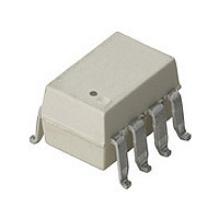
OPTOCOUPLER AMP 100KHZ VDE 8-SMD
Manufacturer
Avago Technologies US Inc.
Datasheet
1.HCPL-7840-000E.pdf
(19 pages)
Specifications of HCPL-7840#360
Amplifier Type
Isolation
Number Of Circuits
1
Output Type
Differential
-3db Bandwidth
100kHz
Current - Input Bias
500nA
Voltage - Input Offset
300µV
Current - Supply
10.9mA
Current - Output / Channel
15.5mA
Voltage - Supply, Single/dual (±)
4.5 V ~ 5.5 V
Operating Temperature
-40°C ~ 85°C
Mounting Type
Surface Mount
Package / Case
8-SMD Gull Wing
Operating Supply Voltage (typ)
5V
Lead Free Status / RoHS Status
Contains lead / RoHS non-compliant
Slew Rate
-
Gain Bandwidth Product
-
Lead Free Status / RoHS Status
Not Compliant, Contains lead / RoHS non-compliant
Available stocks
Company
Part Number
Manufacturer
Quantity
Price


Notes:
General Note: Typical values represent the mean value of all characteriza-
tion units at the nominal operating conditions. Typical drift specifica-
tions are determined by calculating the rate of change of the specified
parameter versus the drift pa-rameter (at nominal operating conditions)
for each characterization unit, and then averaging the individual unit
rates. The corresponding drift figures are normalized to the nominal
operating conditions and show how much drift occurs as the par-ticular
drift parameter is varied from its nominal value, with all other param-
eters held at their nominal operating values. Note that the typical drift
specifications in the tables below may differ from the slopes of the mean
curves shown in the corresponding figures.
10. When the differential input signal exceeds approximately 308 mV,
10
1. Avago recommends operation with
2. This is the Absolute Value of Input Offset Change vs. Temperature.
3. Gain is defined as the slope of the best-fit line of differential output
4. This is the Absolute Value of Gain Change vs. Temperature.
5. Nonlinearity is defined as half of the peak-to-peak output deviation
6. NL
7. The input supply current decreases as the differential input voltage
8. The maximum specified output supply current occurs when the
9. Because of the switched-capacitor nature of the input sigma-delta
Limiting V
ity drift. If V
be activated. This test mode is for testing LED coupling and is not
intended for customer use.
voltage
over the specified input range.
from the best-fit gain line, expressed as a percentage of the full-scale
differential output voltage.
±100 mV.
(V
differential input voltage (V
ommended operat-ing input voltage. However, the out-put supply
current will continue to rise for differential input voltages up to
approximately -300 mV, beyond which the output supply current
remains constant.
con-verter, time-averaged values are shown.
the outputs will limit at the typical values shown.
IN+
100
–V
is the nonlinearity specified over an input voltage range of
IN-
) decreases.
IN+
IN-
to 100 mV will improve DC nonlinearity and nonlinear-
is brought above V
(V
OUT+
–V
OUT-
IN+
) vs. differential input voltage (V
–V
DD1
IN-
) = -200 mV, the maximum rec-
– 2 V, an internal test mode may
V
IN-
= 0 V (tied to GND1).
IN+
–V
IN-
)
11. Short circuit current is the amount of output current generated
12. CMRR is defined as the ratio of the differential signal
13. Output noise comes from two primary sources: chopper noise
14. CMTI (Common Mode Transient Immunity or CMR, Common Mode
15. Data sheet value is the differential amplitude of the transient at the
16. In accordance with UL 1577, each optocoupler is proof tested by ap-
17. The Input-Output Momentary Withstand Voltage is a dielectric
18. This is a two-terminal measurement: pins 1–4 are shorted together
when either output is shorted to V
gain (signal applied differentially between pins 2 and 3)
to the common-mode gain (input pins tied together and the signal
applied to both inputs at the same time), expressed in dB.
and sigma-delta quantization noise. Chopper noise results from
chopper stabilization of the output op-amps. It occurs at a specific
frequency (typically 400 kHz at room temperature), and is not at-
tenuated by the internal output filter. A filter circuit can be easily
added to the external post-amplifier to reduce the total rms output
noise. The internal output filter does eliminate most, but not
all, of the sigma-delta quantization noise. The magnitude of the
output quantization noise is very small at lower frequencies (below
10 kHz) and increases with increasing frequency.
Rejection) is tested by applying an exponentially rising/falling
voltage step on pin 4 (GND1) with respect to pin 5 (GND2). The rise
time of the test waveform is set to approximately 50 ns. The ampli-
tude of the step is adjusted until the differential output (V
exhibits more than a 200 mV deviation from the average output
voltage for more than 1µs. The HCPL-7840 will continue to func-tion
if more than
long as the breakdown voltage limitations are observed.
output of the HCPL-7840 when a 1 V
40 ns rise and fall times is applied to both V
plying an insulation test voltage ≥4500 Vrms for 1 second (leakage
detection current limit, I
100% production test for partial discharge (method b) shown in
IEC/EN/DIN EN 60747-5-2 Insulation Characteristic Table.
voltage rating that should not be interpreted as an input-output
continuous voltage rating. For the continuous voltage rating refer
to the VDE 0884 insulation characteristics table and your equipment
level safety specification.
and pins 5–8 are shorted together.
10 kV/µs common mode slopes are applied, as
I-O
≤ 5 µA). This test is performed before the
DD2
pk-pk
or ground.
, 1 MHz square wave with
DD1
and V
DD2
.
OUT+
–V
OUT-
)
Related parts for HCPL-7840#360
Image
Part Number
Description
Manufacturer
Datasheet
Request
R

Part Number:
Description:
OPTOCOUPLER 2CH 2.5A 16-SOIC
Manufacturer:
Avago Technologies US Inc.
Datasheet:

Part Number:
Description:
OPTOCOUPLER LOG-OUT 10MBD 8SOIC
Manufacturer:
Avago Technologies US Inc.
Datasheet:

Part Number:
Description:
OPTOCOUPLER 1CH 2.5A 8-SMD
Manufacturer:
Avago Technologies US Inc.
Datasheet:

Part Number:
Description:
OPTOCOUPLER 1CH 0.6A 8-DIP
Manufacturer:
Avago Technologies US Inc.
Datasheet:
Part Number:
Description:
OPTOCOUPLER LOG-OUT 10MBD 8-SOIC
Manufacturer:
Avago Technologies US Inc.
Datasheet:

Part Number:
Description:
OPTOCOUPLER 1CH 2.5A 8-DIP
Manufacturer:
Avago Technologies US Inc.
Datasheet:

Part Number:
Description:
OPTOCOUPLER 2CH LOW IF 8-DIP
Manufacturer:
Avago Technologies US Inc.
Datasheet:

Part Number:
Description:
OPTOCOUPLER AMP 100KHZ 8-DIP
Manufacturer:
Avago Technologies US Inc.
Datasheet:
Part Number:
Description:
OPTOCOUPLER GATE DRV 2A 16-SOIC
Manufacturer:
Avago Technologies US Inc.
Datasheet:
Part Number:
Description:
OPTOCOUPLER GATE DRV 2A 16-SOIC
Manufacturer:
Avago Technologies US Inc.
Datasheet:

Part Number:
Description:
OPTOCOUPLER DAA PLC ISO 16SOIC
Manufacturer:
Avago Technologies US Inc.
Datasheet:
Part Number:
Description:
ISOLATOR DIG 100MBD 1CH 8-SOIC
Manufacturer:
Avago Technologies US Inc.
Datasheet:
Part Number:
Description:
ISOLATOR DIG 100MBD 2CH 8-SOIC
Manufacturer:
Avago Technologies US Inc.
Datasheet:
Part Number:
Description:
ISOLATOR DGTL 4CH 100MBD 16-SOIC
Manufacturer:
Avago Technologies US Inc.
Datasheet:
Part Number:
Description:
ISOLATOR HS DIG DUAL BI 8-SOIC
Manufacturer:
Avago Technologies US Inc.
Datasheet: