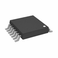
AD8554ARUZ Analog Devices Inc, AD8554ARUZ Datasheet - Page 18

AD8554ARUZ
Manufacturer Part Number
AD8554ARUZ
Description
IC OPAMP CHOPPER R-R 14TSSOP
Manufacturer
Analog Devices Inc
Datasheet
1.AD8551ARMZ-REEL.pdf
(24 pages)
Specifications of AD8554ARUZ
Slew Rate
0.4 V/µs
Amplifier Type
Chopper (Zero-Drift)
Number Of Circuits
4
Output Type
Rail-to-Rail
Gain Bandwidth Product
1.5MHz
Current - Input Bias
10pA
Voltage - Input Offset
1000µV
Current - Supply
850µA
Current - Output / Channel
30mA
Voltage - Supply, Single/dual (±)
2.7 V ~ 5.5 V
Operating Temperature
-40°C ~ 125°C
Mounting Type
Surface Mount
Package / Case
14-TSSOP
Op Amp Type
Zero Drift
No. Of Amplifiers
4
Bandwidth
1.5MHz
Supply Voltage Range
2.7V To 5.5V
Amplifier Case Style
TSSOP
No. Of Pins
14
Lead Free Status / RoHS Status
Lead free / RoHS Compliant
-3db Bandwidth
-
Lead Free Status / RoHS Status
Lead free / RoHS Compliant, Lead free / RoHS Compliant
Available stocks
Company
Part Number
Manufacturer
Quantity
Price
Part Number:
AD8554ARUZ
Manufacturer:
ADI/亚德诺
Quantity:
20 000
Company:
Part Number:
AD8554ARUZ-REEL
Manufacturer:
AD
Quantity:
1 450
AD8551/AD8552/AD8554
BROADBAND AND EXTERNAL RESISTOR NOISE
CONSIDERATIONS
The total broadband noise output from any amplifier is primarily
a function of three types of noise: input voltage noise from the
amplifier, input current noise from the amplifier, and Johnson
noise from the external resistors used around the amplifier.
Input voltage noise, or e
used. The Johnson noise from a resistor is a function of the re-
sistance and the temperature. Input current noise, or i
an equivalent voltage noise proportional to the resistors used
around the amplifier. These noise sources are not correlated
with each other and their combined noise sums in a root-
squared-sum fashion. The full equation is given as
Where:
e
i
R
k = Boltzmann’s constant (1.38 × 10
T = ambient temperature in Kelvin (K = 273.15 + °C).
The input voltage noise density (e
and the input noise, i
the input voltage noise, provided the source resistance is less
than 106 kΩ. With source resistance greater than 106 kΩ, the
overall noise of the system is dominated by the Johnson noise of
the resistor itself.
Figure 59. Reducing Autocorrection Clock Noise Using a Feedback Capacitor
n
n
S
= the input current noise of the amplifier.
= the input voltage noise density of the amplifier.
= source resistance connected to the noninverting terminal.
e
–100
–120
n
–20
–40
–60
–80
_
V
0
TOTAL
Figure 60. Spectral Analysis Using a Feedback Capacitor
IN
0
@ 200Hz
= 1mV rms
1
=
[
e
n
2
2
+
n
4
, is 2 fA/√Hz. The e
kTr
3
n
100Ω
, is strictly a function of the amplifier
FREQUENCY (kHz)
S
+
4
(
i
n
n
R
) of the AD855x is 42 nV/√Hz,
5
S
)
2
−23
100kΩ
]
3.3nF
1
6
2
J/K).
n, TOTAL
7
V
A
SY
V
8
is dominated by
= 60dB
= 5V
9
n
, creates
10
(15)
Rev. D | Page 18 of 24
Because the input current noise of the AD855x is very small,
it does not become a dominant term unless R
4 GΩ, which is an impractical value of source resistance.
The total noise (e
Hertz, and the equivalent rms noise over a certain bandwidth
can be found as
where BW is the bandwidth of interest in Hertz.
OUTPUT OVERDRIVE RECOVERY
The AD855x amplifiers have an excellent overdrive recovery of
only 200 μs from either supply rail. This characteristic is par-
ticularly difficult for autocorrection amplifiers because the
nulling amplifier requires a nontrivial amount of time to error
correct the main amplifier back to a valid output. Figure 29 and
Figure 30 show the positive and negative overdrive recovery
times for the AD855x.
The output overdrive recovery for an autocorrection amplifier is
defined as the time it takes for the output to correct to its final
voltage from an overload state. It is measured by placing the
amplifier in a high gain configuration with an input signal that
forces the output voltage to the supply rail. The input voltage is
then stepped down to the linear region of the amplifier, usually
to halfway between the supplies. The time from the input signal
stepdown to the output settling to within 100 μV of its final
value is the overdrive recovery time.
INPUT OVERVOLTAGE PROTECTION
Although the AD855x is a rail-to-rail input amplifier, exercise
care to ensure that the potential difference between the inputs
does not exceed 5 V. Under normal operating conditions, the
amplifier corrects its output to ensure the two inputs are at the
same voltage. However, if the device is configured as a comparator,
or is under some unusual operating condition, the input voltages
may be forced to different potentials. This can cause excessive
current to flow through internal diodes in the AD855x used to
protect the input stage against overvoltage.
If either input exceeds either supply rail by more than 0.3 V,
large amounts of current begin to flow through the ESD pro-
tection diodes in the amplifier. These diodes connect between
the inputs and each supply rail to protect the input transistors
against an electrostatic discharge event and are normally
reverse-biased. However, if the input voltage exceeds the supply
voltage, these ESD diodes become forward-biased. Without
current limiting, excessive amounts of current can flow through
these diodes, causing permanent damage to the device. If inputs
are subjected to overvoltage, appropriate series resistors should
be inserted to limit the diode current to less than 2 mA maximum.
e
n
=
e
n
,
TOTAL
n, TOTAL
×
BW
) is expressed in volts per square root
S
is greater than
(16)


