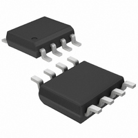
MAX4402ASA+T Maxim Integrated Products, MAX4402ASA+T Datasheet - Page 8

MAX4402ASA+T
Manufacturer Part Number
MAX4402ASA+T
Description
IC OP AMP R-R W/SD 8-SOIC
Manufacturer
Maxim Integrated Products
Datasheet
1.MAX4400AXKT.pdf
(12 pages)
Specifications of MAX4402ASA+T
Amplifier Type
General Purpose
Number Of Circuits
2
Output Type
Rail-to-Rail
Slew Rate
1 V/µs
Gain Bandwidth Product
800kHz
Current - Input Bias
0.1pA
Voltage - Input Offset
1000µV
Current - Supply
410µA
Current - Output / Channel
30mA
Voltage - Supply, Single/dual (±)
2.5 V ~ 5.5 V, ±1.25 V ~ 2.75 V
Operating Temperature
-40°C ~ 125°C
Mounting Type
Surface Mount
Package / Case
8-SOIC (3.9mm Width)
Number Of Channels
2
Voltage Gain Db
120 dB
Common Mode Rejection Ratio (min)
68 dB
Input Offset Voltage
5.5 mV
Operating Supply Voltage
3 V, 5 V
Supply Current
0.14 mA
Maximum Power Dissipation
471 mW
Maximum Operating Temperature
+ 125 C
Mounting Style
SMD/SMT
Minimum Operating Temperature
- 40 C
Lead Free Status / RoHS Status
Lead free / RoHS Compliant
-3db Bandwidth
-
Lead Free Status / Rohs Status
Details
circuit’s response by isolating the load capacitance
from the op amp’s output.
The MAX4401 features a low-power shutdown mode.
When SHDN goes low, the supply current drops to
20pA (typ) and the output enters a high-impedance
state. Pull SHDN high to enable the amplifier. Do not
leave SHDN floating. Figure 4 shows the shutdown
waveform.
The MAX4400–MAX4403 outputs typically settle within
5µs after power-up. Figure 5 shows the output voltage
on power-up and power-down.
Single/Dual/Quad, Low-Cost, Single-Supply,
Rail-to-Rail Op Amps with Shutdown
Figure 2. Small-Signal Transient Response with Excessive
Capacitive Load
Figure 4. Shutdown Waveform
8
_______________________________________________________________________________________
R
C
L
L
= 10MΩ TO GND
= 25pF
Applications Information
400µs/div
2µs/div
Shutdown Mode
SHDN
2V/div
OUT
IN
50mV/div
OUT
Power-Up
The MAX4400–MAX4403 operate from a single +2.5V
to +5.5V power supply. Bypass the power supply with a
0.1µF capacitor to ground.
Good layout techniques optimize performance by
decreasing the amount of stray capacitance at the op
amp’s inputs and outputs. To decrease stray capaci-
tance, minimize trace lengths by placing external com-
ponents close to the op amp’s pins.
Figure 3. Capacitive-Load-Driving Circuit
Figure 5. Power-Up/Power-Down Waveform
MAX4400/MAX4401 TRANSISTOR COUNT: 101
MAX4402 TRANSISTOR COUNT: 202
MAX4403 TRANSISTOR COUNT: 404
2V/div
1V/div
OUT
V
DD
Power Supplies and Layout
MAX4400
MAX4401
MAX4402
MAX4403
10µs/div
Chip Information
R
ISO
C
L


