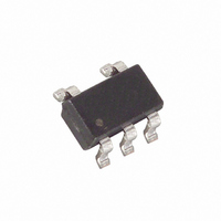
MAX4493AUK+T Maxim Integrated Products, MAX4493AUK+T Datasheet - Page 8

MAX4493AUK+T
Manufacturer Part Number
MAX4493AUK+T
Description
IC OP AMP GP SGL LP SOT23-5
Manufacturer
Maxim Integrated Products
Datasheet
1.MAX4493AXKT.pdf
(15 pages)
Specifications of MAX4493AUK+T
Amplifier Type
General Purpose
Number Of Circuits
1
Output Type
Rail-to-Rail
Slew Rate
3 V/µs
Gain Bandwidth Product
5MHz
Current - Input Bias
200nA
Voltage - Input Offset
300µV
Current - Supply
770µA
Current - Output / Channel
15mA
Voltage - Supply, Single/dual (±)
4.5 V ~ 11 V, ±2.25 V ~ 5.5 V
Operating Temperature
-40°C ~ 125°C
Mounting Type
Surface Mount
Package / Case
SOT-23-5, SC-74A, SOT-25
Number Of Channels
1
Voltage Gain Db
110 dB
Common Mode Rejection Ratio (min)
65 dB
Input Offset Voltage
5 mV
Operating Supply Voltage
5 V, 9 V
Maximum Power Dissipation
571 mW
Maximum Operating Temperature
+ 125 C
Mounting Style
SMD/SMT
Maximum Dual Supply Voltage
+/- 5.5 V
Minimum Operating Temperature
- 40 C
Lead Free Status / RoHS Status
Lead free / RoHS Compliant
-3db Bandwidth
-
Lead Free Status / Rohs Status
Details
where the slew rate (SR) is 3V/µs. Figure 2 shows the
full-power bandwidth as a function of the peak-to-peak
AC output voltage.
The MAX4493/MAX4494/MAX4495 typically settle within
3µs after power-up. See Power-Up Time in Typical
Operating Characteristics .
The MAX4493/MAX4494/MAX4495 operate with dual
supplies from ±2.25V to ±5.5V. Bypass both V
V
Good layout technique helps optimize performance by
decreasing the amount of stray capacitance at the op
amp’s inputs and outputs. To decrease stray capaci-
tance, minimize trace lengths by placing external com-
ponents close to the op amp’s pins.
SC70, Low-Power, General-Purpose,
Dual-Supply, Rail-to-Rail Op Amps
8
EE
_______________________________________________________________________________________
with their own 0.1µF capacitor to ground.
0.1μF
0.1μF
TOP VIEW
+5V
-5V
DAC
REF
Typical Operating Circuit
OUTA
INA+
INA-
V
R
EE
g
Power Supplies and Layout
1
2
4
3
SO/SOT23/μMAX
MAX4494
Power-Up Conditions
MAX4493
+5V
-5V
8
7
6
5
V
OUTB
INB-
INB+
R
CC
f
0.1μF
0.1μF
R
ISO
CC
V
and
OUT
Figure 2. Bandwidth vs. Peak-to-Peak AC Voltage Plot
PROCESS: Bipolar
TOP VIEW
Pin Configurations (continued)
100M
100k
10M
1M
0
OUTA
OUTB
INA+
INB+
vs. OUTPUT VOLTAGE SWING
INA-
INB-
V
CC
1
1
2
3
4
5
6
7
BANDWIDTH
V
2
OUT
SO/TSSOP
MAX4495
(Vp-p)
Chip Information
A
3
V
= +1V/V
4
14
13
12
11
10
9
8
OUTD
IND-
IND+
V
INC+
INC-
OUTC
EE
5


