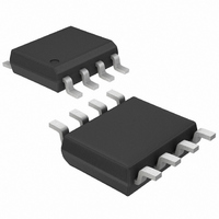
MAX410BESA Maxim Integrated Products, MAX410BESA Datasheet - Page 2

MAX410BESA
Manufacturer Part Number
MAX410BESA
Description
IC OPAMP LN LV PREC 28MHZ 8-SOIC
Manufacturer
Maxim Integrated Products
Datasheet
1.MAX410CSA.pdf
(13 pages)
Specifications of MAX410BESA
Amplifier Type
General Purpose
Number Of Circuits
1
Slew Rate
4.5 V/µs
Gain Bandwidth Product
28MHz
Current - Input Bias
80nA
Voltage - Input Offset
120µV
Current - Supply
2.5mA
Current - Output / Channel
35mA
Voltage - Supply, Single/dual (±)
4.8 V ~ 10.5 V, ±2.4 V ~ 5.25 V
Operating Temperature
-40°C ~ 85°C
Mounting Type
Surface Mount
Package / Case
8-SOIC (3.9mm Width)
Lead Free Status / RoHS Status
Contains lead / RoHS non-compliant
Output Type
-
-3db Bandwidth
-
ABSOLUTE MAXIMUM RATINGS
Supply Voltage .......................................................................12V
Differential Input Current (Note 1) ....................................±20mA
Input Voltage Range........................................................V+ to V-
Common-Mode Input Voltage ..............(V+ + 0.3V) to (V- - 0.3V)
Short-Circuit Current Duration....................................Continuous
Continuous Power Dissipation (T
MAX410/MAX412
Single/Dual/Quad, 28MHz, Low-Noise,
Low-Voltage, Precision Op Amps
ELECTRICAL CHARACTERISTICS
(V+ = 5V, V- = -5V, T
Note 1: The amplifier inputs are connected by internal back-to-back clamp diodes. In order to minimize noise in the input stage, current-
Stresses beyond those listed under “Absolute Maximum Ratings” may cause permanent damage to the device. These are stress ratings only, and functional
operation of the device at these or any other conditions beyond those indicated in the operational sections of the specifications is not implied. Exposure to
absolute maximum rating conditions for extended periods may affect device reliability.
2
Input Offset Voltage
Input Bias Current
Input Offset Current
Differential Input Resistance
Common-Mode Input Resistance
Input Capacitance
Input Noise-Voltage Density
Input Noise-Current Density
Common-Mode Input Voltage
Common-Mode Rejection Ratio
Power-Supply Rejection Ratio
Large-Signal Gain
Output Voltage Swing
Short-Circuit Output Current
Slew Rate
Unity-Gain Bandwidth
Settling Time
Channel Separation
8-Pin Plastic DIP (derate 9.09mW/°C above +70°C) ...727mW
8-Pin SO (derate 5.88mW/°C above +70°C)................471mW
8-Pin TDFN (derate 18.5mW/°C above +70°C) .........1482mW
_______________________________________________________________________________________
limiting resistors are not used. If differential input voltages exceeding ±1.0V are applied, limit input current to 20mA.
PARAMETER
A
= +25°C, unless otherwise noted.)
A
= +70°C)
SYMBOL
R
R
CMRR
PSRR
A
V
GBW
IN(CM)
IN(Diff)
V
V
C
I
I
SR
C
e
VOL
OUT
I
OS
i
CM
SC
t
OS
B
n
IN
S
n
S
MAX410, MAX410B, MAX412, MAX412B
MAX414, MAX414B
MAX410, MAX412,
MAX414
MAX410B, MAX412B,
MAX414B
f
f
V
V
R
R
R
10kΩ || 20pF load
10kΩ || 20pF load
To 0.1%
f
O
O
O
CM
S
L
L
L
= 10Hz
= 1000Hz
= 1kHz
= ±2.4V to ±5.25V
= 2kΩ, V
= 600Ω, V
= 2kΩ
= ±3.5V
O
O
= ±3.6V
CONDITIONS
= ±3.5V
MAX414
Operating Temperature Ranges:
Storage Temperature Range .............................-65°C to +150°C
Lead Temperature (soldering, 10s) .................................+300°C
14-Pin Plastic DIP (derate 10.00mW/°C above +70°C)800mW
14-Pin SO (derate 8.33mW/°C above +70°C)..............667mW
MAX41_C_ _ .......................................................0°C to +70°C
MAX41_E_ _.....................................................-40°C to +85°C
MAX41_M_ _ ..................................................-55°C to +125°C
10Hz
1000Hz (Note 2)
1000Hz (Note 2)
±3.5
+3.6
MIN
115
115
110
-3.7
96
±120
±150
+3.7/
+3.7/
TYP
±80
±40
-3.8
122
120
-3.8
135
130
103
1.5
2.4
2.6
1.2
4.5
1.3
20
40
35
28
4
7
±250
±320
±150
MAX
±80
2.4
4.0
UNITS
pA√Hz
nV√Hz
MHz
V/µs
MΩ
mA
kΩ
dB
dB
dB
dB
µV
nA
nA
pF
µs
V
V


