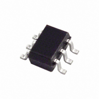
AD8029AKS-R2 Analog Devices Inc, AD8029AKS-R2 Datasheet - Page 6

AD8029AKS-R2
Manufacturer Part Number
AD8029AKS-R2
Description
IC AMP GP R-R LP 170MA SC70-6
Manufacturer
Analog Devices Inc
Datasheet
1.AD8029ARZ.pdf
(20 pages)
Specifications of AD8029AKS-R2
Rohs Status
RoHS non-compliant
Amplifier Type
General Purpose
Number Of Circuits
1
Output Type
Rail-to-Rail
Slew Rate
63 V/µs
-3db Bandwidth
125MHz
Current - Input Bias
1.7µA
Voltage - Input Offset
2000µV
Current - Supply
1.4mA
Current - Output / Channel
170mA
Voltage - Supply, Single/dual (±)
2.7 V ~ 12 V, ±1.35 V ~ 6 V
Operating Temperature
-40°C ~ 125°C
Mounting Type
Surface Mount
Package / Case
SC-70-6, SC-88, SOT-363
Gain Bandwidth Product
-
Other names
AD8029AKS-R2TR
AD8029/AD8030/AD8040
ABSOLUTE MAXIMUM RATINGS
Table 4. AD8029/AD8030/AD8040 Stress Ratings
Parameter
Supply Voltage
Power Dissipation
Common-Mode Input Voltage
Differential Input Voltage
Storage Temperature
Operating Temperature Range
Lead Temperature Range
Junction Temperature
Stresses above those listed under Absolute Maximum Ratings
may cause permanent damage to the device. This is a stress
rating only; functional operation of the device at these or any
other conditions above those indicated in the operational
section of this specification is not implied. Exposure to absolute
maximum rating conditions for extended periods may affect
device reliability.
MAXIMUM POWER DISSIPATION
The maximum safe power dissipation in the AD8029/AD8030/
AD8040 package is limited by the associated rise in junction
temperature (T
locally reaches the junction temperature. At approximately
150°C, which is the glass transition temperature, the plastic
changes its properties. Even temporarily exceeding this
temperature limit may change the stresses that the package
exerts on the die, permanently shifting the parametric
performance of the AD8029/AD8030/AD8040. Exceeding a
junction temperature of 175°C for an extended period can
result in changes in silicon devices, potentially causing failure.
The still-air thermal properties of the package and PCB (θ
ambient temperature (T
package (P
junction temperature can be calculated as
The power dissipated in the package (P
quiescent power dissipation and the power dissipated in the
package due to the load drive for all outputs. The quiescent
power is the voltage between the supply pins (V
quiescent current (I
midsupply, the total drive power is V
dissipated in the package and some in the load (V
The difference between the total drive power and the load
power is the drive power dissipated in the package.
(Soldering 10 sec)
D
) determine the junction temperature of the die. The
J
) on the die. The plastic encapsulating the die
S
). Assuming the load (R
T
A
J
), and the total power dissipated in the
= T
A
+ (P
D
× θ
Rating
12.6 V
See Figure 6
±V
±1.8 V
–65°C to +125°C
–40°C to +125°C
300°C
150°C
S
/2 × I
S
D
JA
) is the sum of the
± 0.5 V
)
OUT
L
) is referenced to
, some of which is
S
) times the
OUT
× I
OUT
JA
).
),
Rev. A | Page 6 of 20
RMS output voltages should be considered. If R
V
V
If the rms signal levels are indeterminate, consider the worst
case, when V
In single-supply operation with R
is V
Airflow will increase heat dissipation, effectively reducing θ
Also, more metal directly in contact with the package leads
from metal traces, through holes, ground, and power planes will
reduce the θ
tances at the input leads of high speed op amps, as discussed in
the PCB Layout section.
Figure 6 shows the maximum safe power dissipation in the
package versus the ambient temperature for the SOIC-8
(125°C/W), SOT23-8 (160°C/W), SOIC-14 (90°C/W),
TSSOP-14 (120°C/W), and SC70-6 (208°C/W) packages on a
JEDEC standard 4-layer board. θ
Output Short Circuit
Shorting the output to ground or drawing excessive current
from the AD8029/AD8030/AD8040 could cause catastrophic
failure.
S
S
–, as in single-supply operation, then the total drive power is
× I
P
OUT
D
OUT
= Quiescent Power + (Total Drive Power – Load Power)
2.5
2.0
1.5
1.0
0.5
= V
0
–40
.
S
–30
SOT-23-8
/2.
SC70-6
JA
SOIC-8
P
OUT
. Care must be taken to minimize parasitic capaci-
D
–20 –10
=
Figure 6. Maximum Power Dissipation
= V
(
TSSOP-14
V
S
S
P
0 10 20 30 40 50 60 70 80 90 100 110 120
/4 for R
D
×
AMBIENT TEMPERATURE (°C)
I
=
S
SOIC-14
(
)
V
+
S
L
⎛
⎜
⎜
⎝
×
to midsupply:
V
2
I
S
S
JA
×
) (
L
+
referenced to V
values are approximations.
V
OUT
R
V
L
S
R
4 /
L
⎞
⎟
⎟
⎠
)
2
–
V
OUT
R
L
L
is referenced to
2
S
–, worst case
JA
.


