AD521JD Analog Devices Inc, AD521JD Datasheet - Page 3
AD521JD
Manufacturer Part Number
AD521JD
Description
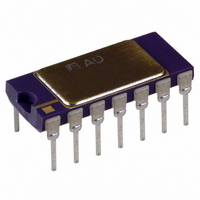
IC AMP INST 40MHZ PREC LN 14CDIP
Manufacturer
Analog Devices Inc
Datasheet
1.AD521JDZ.pdf
(6 pages)
Specifications of AD521JD
Mounting Type
Through Hole
Rohs Status
RoHS non-compliant
Amplifier Type
Instrumentation
Number Of Circuits
1
Slew Rate
10 V/µs
-3db Bandwidth
2MHz
Current - Input Bias
80nA
Voltage - Input Offset
3000µV
Current - Supply
5mA
Voltage - Supply, Single/dual (±)
±5 V ~ 18 V
Operating Temperature
0°C ~ 70°C
Package / Case
14-CDIP (0.300", 7.62mm)
No. Of Amplifiers
1
Bandwidth
2MHz
Amplifier Case Style
DIP
No. Of Pins
14
Programmable Gain Max
1000
Supply Voltage Min
5V
Peak Reflow Compatible (260 C)
No
Output Type
-
Current - Output / Channel
-
Gain Bandwidth Product
-
Lead Free Status / RoHS Status
Contains lead / RoHS non-compliant
Available stocks
Company
Part Number
Manufacturer
Quantity
Price

Part Number:
AD521JD
Manufacturer:
ADI/亚德诺
Quantity:
20 000
Company:
Part Number:
AD521JDZ
Manufacturer:
Analog Devices Inc
Quantity:
135


ential signal of greater than 11V is applied between the inputs,
transistor clamps are activated which drop the exces!' input
voltage across internal input resistors. If a continuous overload
is maintained, power dissipated in these resistors causes temper-
atUre gradients and a corresponding change in offset voltage,
as well as added thermal time constant, but will not damage
the device.)
swing, distortion may increase to as much as 0.3%.
amplifier will produce full output swing.
4. Differential Overload Recovery is the time it takes the ampli-
fier to recover from a pulsed 30V differential input with 15V
of common mode voltage, to within 10mV of final value. The
justing the gain setting resistors. (Input voltage should be re-
2. Nonlinearity is defined as the ratio of the deviation from
the "best straight line" through a full scale output range of
1:9volts. With a combination of high gain and :tlO volt output
3. Full Peak Response is the frequency below which a typical
test input is a 30V, 10,us pulse at a 1kHz rate. (When a differ-
test input is 30V, 10,us pulse at a 1kHz rate. (When a com-
[
NOTES:
stricted to :t10V for gains equal to or less than 1.)
5. Common Mode Step Recovery is the time it takes the amp-
lifier to recover from a 30V common mode input with zero
volts of differential signal to within 10mV of final value. The
Model
AD52lJD
AD52IKD
AD521LD
AD521SD
AD521SD/883B2 - 55°C to + 125°C 14-Pin Ceramic DIP D-14
AD52lJ Chips
AD521K Chips
AD521S Chips
NOTES
IFor outline information see Package Information
2Standard military drawing available.
8BLA
1. Gains below 1 and above 1000 are obtained by simply ad-
DoC to + 7DoC
DoC to + 7DoC
Temperature
Range
DoC to + 7DoC
DoC to + 7DoC
DoC to + 7DoC
- 55°C to + 125°C 14-Pin Ceramic DIP D-14
- 55°C to + 125°C Die
ORDERING GUIDE
Description
Die
Die
14-Pin Ceramic DIP D-14
14-Pin Ceramic DIP D-14
14-Pin Ceramic DIP D-14
section.
Package
Option!
constant, but will not damage the device.)
mon mode signal greater than Vs -o.5V is applied to the
inputs, transistor clamps are activated which drop the excessive
input voltage across internal input resistors. Power dissipated
in these resistors causes temperatUre gradients and a correspon-
ding change in offset voltage, as well as an added thermal time
6. Output Offset Voltage versus Power Supply includes a
constant 0.005 times the unnulled output offset per percent
change in either power supply. If the output offset is nulled,
either input to the power supplies.
the maximum peak-to-peak voltage noise ovserved during 2
of 3 separate 10 second periods with the test circuit of Fig-
ure 8.
the output offset change versus supply change is substantially
reduced.
7. Differential Input Impedance is the impedance between the
8. Common Mode Input Impedance is the impedance from
9. Maximum Input Voltage (differential or at either input) is
that neither input may exceed either supply (even when
Vs
two inputs must not exceed 30V. (See also Notes 4 and 5.)
10. O.lHz to 10Hz Peak-to-Peak Voltage Noise is defined as
two inputs.
30V when using :t15V supplies. A more general specification is
+INPUT
RGAIN
=
14
1
0) by more than 15V and that the difference
~
R GAIN
METALIZATION
2
Dimensions shown in inches and (mm).
Contact factory for latest dimensions.
0.110 {2.8001
3
-INPUT
fN~TRf !MFNTA TfnN
OFFSET
TRIM
Applying t he AD521
4
PHOTOGRAPH
-Vs
5
6
OFFSET
TRIM
AMP! !FfFR.C; 4-,ffl;
between
the
a
Related parts for AD521JD
Image
Part Number
Description
Manufacturer
Datasheet
Request
R

Part Number:
Description:
±1.7g Dual-Axis IMEMS Accelerometer Evaluation Board
Manufacturer:
Analog Devices Inc
Datasheet:

Part Number:
Description:
Inertial Sensor Evaluation System
Manufacturer:
Analog Devices Inc
Datasheet:
Part Number:
Description:
Manufacturer:
Analog Devices Inc
Datasheet:
Part Number:
Description:
Manufacturer:
Analog Devices Inc
Datasheet:
Part Number:
Description:
Manufacturer:
Analog Devices Inc
Datasheet:
Part Number:
Description:
Manufacturer:
Analog Devices Inc
Datasheet:
Part Number:
Description:
Manufacturer:
Analog Devices Inc
Datasheet:
Part Number:
Description:
Manufacturer:
Analog Devices Inc
Datasheet:
Part Number:
Description:
Manufacturer:
Analog Devices Inc
Datasheet:
Part Number:
Description:
Manufacturer:
Analog Devices Inc
Datasheet:
Part Number:
Description:
Manufacturer:
Analog Devices Inc
Datasheet:
Part Number:
Description:
Manufacturer:
Analog Devices Inc
Datasheet:
Part Number:
Description:
Manufacturer:
Analog Devices Inc
Datasheet: