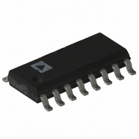
AD8594AR-REEL7 Analog Devices Inc, AD8594AR-REEL7 Datasheet - Page 12

AD8594AR-REEL7
Manufacturer Part Number
AD8594AR-REEL7
Description
IC OPAMP GP R-R CMOS 3MHZ 16SOIC
Manufacturer
Analog Devices Inc
Datasheet
1.AD8592ARMZ-REEL.pdf
(16 pages)
Specifications of AD8594AR-REEL7
Rohs Status
RoHS non-compliant
Amplifier Type
General Purpose
Number Of Circuits
4
Output Type
Rail-to-Rail
Slew Rate
5 V/µs
Gain Bandwidth Product
3MHz
Current - Input Bias
5pA
Voltage - Input Offset
2000µV
Current - Supply
1.25mA
Current - Output / Channel
250mA
Voltage - Supply, Single/dual (±)
2.5 V ~ 6 V
Operating Temperature
-40°C ~ 85°C
Mounting Type
Surface Mount
Package / Case
16-SOIC (3.9mm Width)
-3db Bandwidth
-
AD8591/AD8592/AD8594
In any application, the absolute maximum junction temperature
must be limited to 150°C. If the junction temperature is exceeded,
the device could suffer premature failure. If the output voltage
and output current are in phase, for example, with a purely resistive
load, the power dissipated by the AD859x can be found as
where:
I
V
V
By calculating the power dissipation of the device and using the
thermal resistance value for a given package type, the maximum
allowable ambient temperature for an application can be found
using Equation 3.
CAPACITIVE LOADING
The AD859x exhibits excellent capacitive load driving capabilities
and can drive to 10 nF directly. Although the device is stable
with large capacitive loads, there is a decrease in amplifier
bandwidth as the capacitive load increases. Figure 35 shows
a graph of the AD8592 unity-gain bandwidth under various
capacitive loads.
When driving heavy capacitive loads directly from the AD859x
output, a snubber network can be used to improve the transient
response. This network consists of a series RC connected from
the output of the amplifier to ground, placing it in parallel with
the capacitive load. The configuration is shown in Figure 36.
Although this network does not increase the bandwidth of the
amplifier, it significantly reduces the amount of overshoot, as
shown in Figure 37.
Figure 36. Configuration for Snubber Network to Compensate for Capacitive Loads
LOAD
SY
OUT
is the AD859x supply voltage.
P
is the AD859x output load current.
is the output voltage.
DISS
4.0
3.5
3.0
2.5
2.0
1.5
1.0
0.5
0
0.01
= I
Figure 35. Unity-Gain Bandwidth vs. Capacitive Load
100mV p-p
LOAD
× ( V
V
IN
0.1
SY
− V
AD8592
CAPACITIVE LOAD (nF)
+5V
OUT
)
1
R
5Ω
C
1µF
S
S
C
47nF
L
10
V
OUT
V
R
T
S
A
L
= ±2.5V
= 1kΩ
= 25°C
100
Rev. B | Page 12 of 16
(4)
The optimum values for the snubber network should be
determined empirically based on the size of the capacitive load.
Table 5 shows a few sample snubber network values for a given
load capacitance.
Table 5. Snubber Networks for Large Capacitive Loads
Load Capacitance, C
0.47
4.7
47
PC98-COMPLIANT HEADPHONE/SPEAKER
AMPLIFIER
Because of its high output current performance and shutdown
feature, the AD8592 makes an excellent amplifier for driving an
audio output jack in a computer application. Figure 38 shows
how the AD8592 can be interfaced with an AC’97 codec to
drive headphones or speakers.
LINE_OUT_R
LINE_OUT_L
*ADDITIONAL PINS OMITTED FOR CLARITY.
AD1881A*
47nF LOAD
IN CIRCUIT
SNUBBER
(AC’97)
AV
AV
AV
ONLY
Figure 37. Snubber Network Reduces Overshoot and Ringing
Figure 38. PC98-Compliant Headphone/Line Out Amplifier
DD1
DD2
SS1
25
38
35
36
26
+5V
Caused by Driving Heavy Capacitive Loads
2
3
7
8
50mV
50mV
5
L
6
U1-A
U1-B
(nF)
+5V
10
4
U1 = AD8592
100kΩ
9
1
R1
+5V
100µF
100µF
C1
C2
R
300
30
5
S
(Ω)
Snubber Network
R2
2kΩ
R3
2kΩ
20Ω
20Ω
R5
R4
NC
10µs
C
0.1
1
1
S
(μF)


