ADEL2020AR-20 Analog Devices Inc, ADEL2020AR-20 Datasheet
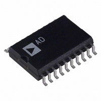
IC OPAMP CF LN LP 60MA 20SOIC

ADEL2020AR-20

Manufacturer Part Number
ADEL2020AR-20
Description
IC OPAMP CF LN LP 60MA 20SOIC
Manufacturer
Analog Devices Inc
Datasheet

Specifications of ADEL2020AR-20

Rohs Status
RoHS non-compliant
Amplifier Type
Current Feedback
Number Of Circuits
1
Slew Rate
500 V/µs
-3db Bandwidth
90MHz
Current - Input Bias
1µA
Voltage - Input Offset
1500µV
Current - Supply
6.8mA
Current - Output / Channel
60mA
Voltage - Supply, Single/dual (±)
6 V ~ 36 V, ±3 V ~ 18 V
Operating Temperature
-40°C ~ 85°C
Mounting Type
Surface Mount
Package / Case
20-SOIC (7.5mm Width)
Output Type
-
Gain Bandwidth Product
-

Available stocks

Company
Part Number
Manufacturer
Quantity
Price
Part Number:
ADEL2020AR-20
Manufacturer:
ADI/亚德诺
Quantity:
20 000
GENERAL DESCRIPTION
The ADEL2020 is an improved second source to the EL2020.
This op amp improves on all the key dynamic specifications
while offering lower power and lower cost. The ADEL2020
offers 50% more bandwidth and gain flatness of 0.1 dB to
beyond 25 MHz. In addition, differential gain and phase are
less than 0.05% and 0.05° while driving one back terminated
cable (150 Ω).
REV. A
Information furnished by Analog Devices is believed to be accurate and
reliable. However, no responsibility is assumed by Analog Devices for its
use, nor for any infringements of patents or other rights of third parties that
may result from its use. No license is granted by implication or otherwise
under any patent or patent rights of Analog Devices. Trademarks and
registered trademarks are the property of their respective companies.
Figure 1. Fine-Scale Gain (Normalized) vs. Frequency
for Various Supply Voltages, R
FEATURES
Ideal for Video Applications
High Speed
Low Noise
Low Power
High Performance Disable Function
0.02% Differential Gain
0.04 Differential Phase
0.1 dB Bandwidth to 25 MHz (G = +2)
90 MHz Bandwidth (–3 dB)
500 V/ s Slew Rate
60 ns Settling Time to 0.1% (V
2.9 nV/√Hz Input Voltage Noise
6.8 mA Supply Current
2.1 mA Supply Current (Power-Down Mode)
Turn-Off Time of 100 ns
Input to Output Isolation of 54 dB (Off State)
+0.1
–0.1
+0.1
–0.1
100k
0
0
1M
FREQUENCY – Hz
R
R
L
L
= 1k
= 150
F
= 750 Ω , Gain = +2
O
10M
= 10 V Step)
15V
5V
15V
5V
100M
The ADEL2020 offers other significant improvements. The
most important is lower power supply current (33% less than the
competition) with higher output drive. Important specifications
like voltage noise and offset voltage are less than half of those
for the EL2020. The ADEL2020 also provides an improved
disable feature. The disable time (to high output impedance) is
100 ns with guaranteed break before make. The ADEL2020 is
offered for the industrial temperature range of –40°C to +85°C
and comes in both PDIP and SOIC packages.
One Technology Way, P.O. Box 9106, Norwood, MA 02062-9106, U.S.A.
Tel: 781/329-4700
Fax: 781/326-8703
Figure 2. Differential Gain and Phase vs. Supply Voltage
BAL
–IN
+IN
V–
0.10
0.09
0.08
0.07
0.06
0.05
0.04
0.03
0.02
0.01
8-Lead PDIP (N)
0
1
2
3
4
5
ADEL2020
GAIN = +2
R
R
f
100 IRE
MODULATED RAMP
TOP VIEW
C
F
L
= 3.58MHz
= 750
= 150
Improved Second Source
6
CONNECTION DIAGRAMS
GAIN
7
8
7
6
5
© 2003 Analog Devices, Inc. All rights reserved.
8
DISABLE
V+
OUTPUT
BAL
SUPPLY VOLTAGE –
9
PHASE
10
BAL
11
–IN
+IN
NC
NC
NC
NC
NC
NC
V–
to the EL2020
20-Lead SOIC (R)
10
NC = NO CONNECT
ADEL2020
1
2
3
4
5
6
7
8
9
12
V
ADEL2020
TOP VIEW
13
www.analog.com
14
20
19
18
17
16
15
14
13
12
11
15
NC
DISABLE
NC
V+
NC
OUTPUT
NC
BAL
NC
NC
0.20
0.18
0.16
0.14
0.12
0.10
0.08
0.06
0.04
0.02
0

Related parts for ADEL2020AR-20

ADEL2020AR-20 Summary of contents

Page 1

FEATURES Ideal for Video Applications 0.02% Differential Gain 0.04 Differential Phase 0.1 dB Bandwidth to 25 MHz (G = +2) High Speed 90 MHz Bandwidth (–3 dB) 500 V/ s Slew Rate 60 ns Settling Time to 0.1% (V Low ...

Page 2

ADEL2020–SPECIFICATIONS Parameter INPUT OFFSET VOLTAGE Offset Voltage Drift COMMON-MODE REJECTION V OS ± Input Current POWER SUPPLY REJECTION V OS ± Input Current INPUT BIAS CURRENT INPUT CHARACTERISTICS +Input Resistance –Input Resistance +Input Capacitance OPEN-LOOP TRANSRESISTANCE OPEN-LOOP DC VOLTAGE GAIN ...

Page 3

... Figure 3. Offset Null Configuration Model ADEL2020AN ADEL2020AR-20 ADEL2020AR-20-REEL CAUTION ESD (electrostatic discharge) sensitive device. Electrostatic charges as high as 4000 V readily accumulate on the human body and test equipment and can discharge without detection. Although the ADEL2020 features proprietary ESD protection circuitry, permanent damage may occur on devices subjected to high energy electrostatic discharges ...

Page 4

ADEL2020–Typical Performance Characteristics PHASE 1 0 –1 GAIN – 15V S –3 5V –4 – FREQUENCY – MHz TPC 1. Closed-Loop Gain and Phase vs. Frequency, = 150 Ω Ω for ...

Page 5

PHASE GAIN 15V 100 FREQUENCY – MHz TPC 7. Closed-Loop Gain and Phase vs. Frequency, = 150 Ω 750 Ω for ± ...

Page 6

ADEL2020 15V OUTPUT LEVEL FOR 3% THD 100k 1M FREQUENCY – Hz TPC 13. Maximum Undistorted Output Voltage vs. Frequency 715 F A ...

Page 7

S 0 – 2 ADEL2020 0 –V S Figure 5. Connection Diagram for A 681 +V S 0.1 F 681 7 V – ADEL2020 3 + ...

Page 8

ADEL2020 GENERAL DESIGN CONSIDERATIONS The ADEL2020 is a current feedback amplifier optimized for use in high performance video and data acquisition systems. Since it uses a current feedback architecture, its closed-loop bandwidth depends on the value of the feedback resistor. ...

Page 9

COPLANARITY 0.10 REV. A OUTLINE DIMENSIONS 8-Lead Plastic Dual-in-Line Package [PDIP] (N-8) Dimensions shown in inches and (millimeters) 0.375 (9.53) 0.365 (9.27) 0.355 (9.02) ...

Page 10

ADEL2020 Revision History Location 1/03—Data Sheet changed from REV REV. A. Format updated . . . . . . . . . . . . . . . . . . . . . . . . . ...

Page 11

–11– ...

Page 12

–12– ...

Related keywords