AD8390ARCZ Analog Devices Inc, AD8390ARCZ Datasheet
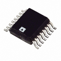
IC AMP DIFF LP LDIST 16QSOP

AD8390ARCZ

Manufacturer Part Number
AD8390ARCZ
Description
IC AMP DIFF LP LDIST 16QSOP
Manufacturer
Analog Devices Inc
Type
Low Powerr
Datasheets

Specifications of AD8390ARCZ

Amplifier Type
Differential
Number Of Circuits
1
Output Type
Differential
Slew Rate
300 V/µs
-3db Bandwidth
60MHz
Current - Input Bias
4µA
Voltage - Input Offset
1000µV
Current - Supply
10mA
Current - Output / Channel
400mA
Voltage - Supply, Single/dual (±)
10 V ~ 24 V, ±5 V ~ 12 V
Operating Temperature
-40°C ~ 85°C
Mounting Type
Surface Mount
Package / Case
16-QSOP Exposed Pad, 16-eQSOP , 16-HQSOP
Common Mode Rejection Ratio
64
Current, Input Bias
-4 μA
Current, Input Offset
±0.05 μA
Current, Output
400 mA
Current, Supply
5.2 mA
Harmonic Distortion
-82 dBc (Second Harmonic), -91 dBc (Third Harmonic)
Impedance, Thermal
44.3 °C/W
Package Type
QSOP/EP-16
Resistance, Input
400 Kilohms
Temperature, Operating, Range
-40 to +85 °C
Voltage, Input
-11 to +10 V
Voltage, Input Offset
±1 mV
Voltage, Noise
8 nV/sqrt Hz
Voltage, Output Swing
44.2 V
Voltage, Supply
10 to 24 V
Lead Free Status / RoHS Status
Lead free / RoHS Compliant
Gain Bandwidth Product
-
Lead Free Status / Rohs Status
RoHS Compliant part Electrostatic Device
FEATURES
Voltage feedback amplifier
Low power operation
High output voltage and current drive
Low distortion
High speed: 300 V/µs differential slew rate
APPLICATIONS
ADSL/ADSL2+ CO and CPE line drivers
xDSL line driver
High current differential amplifiers
GENERAL DESCRIPTION
The AD8390 is a high output current, low power consumption
differential amplifier. It is particularly well suited for the central
office (CO) driver interface in digital subscriber line systems
such as ADSL and ADSL2+. While in full bias operation, the
driver is capable of providing 24.4 dBm output power into low
resistance loads. This is enough to power a 20.4 dBm line while
compensating for losses due to hybrid insertion, transformer
insertion, and back termination resistors.
The AD8390 fully differential amplifier is available in a ther-
mally enhanced lead frame chip scale package (LFCSP-16) and
a 16-lead QSOP/EP. Significant control and flexibility in bias
current have been designed into the AD8390. The four power
modes are controlled by two digital bits,
provide three levels of driver bias and one powered-down state.
In addition, the I
trimming to tailor the performance of
the AD8390.
Rev. C
Information furnished by Analog Devices is believed to be accurate and reliable.
However, no responsibility is assumed by Analog Devices for its use, nor for any
infringements of patents or other rights of third parties that may result from its use.
Specifications subject to change without notice. No license is granted by implication
or otherwise under any patent or patent rights of Analog Devices. Trademarks and
registered trademarks are the property of their respective owners.
Ideal for ADSL and ADSL2+ central office (CO) and
Enables high current differential applications
Single- or dual-power supply operation from 10 V (±5 V)
4 mA total quiescent supply current for full power ADSL
Adjustable supply current to minimize power
400 mA peak output drive current
44.2 V p-p differential output voltage
–82 dBc @ 1 MHz second harmonic
–91 dBc @ 1 MHz third harmonic
customer premises equipment (CPE) applications
up to 24 V (±12 V)
and ADSL2+ CO applications
consumption
ADJ
pin can be used for fine quiescent current
PWDN (1,0
) which
Low Power, High Output Current
The low power consumption, high output current, high output
voltage swing, and robust thermal packaging enable the AD8390
to be used as the central office line driver in ADSL, ADSL2+,
and proprietary xDSL systems, as well as in other high current
applications requiring a differential amplifier.
One Technology Way, P.O. Box 9106, Norwood, MA 02062-9106, U.S.A.
Tel: 781.329.4700
Fax: 781.326.8703
PWDN1
PWDN0
PWDN1
PWDN0
+IN
–IN
DGND
V
OCM
+IN
–IN
NC = NO CONNECT
NC
NC
1
4
NC = NO CONNECT
Figure 1. 4 mm × 4 mm 16-Lead LFCSP
PIN CONFIGURATIONS
1
8
NC
NC
16
5
© 2004 Analog Devices, Inc. All rights reserved.
Differential Amplifier
Figure 2. 16-Lead QSOP/EP
DGND
V
OCM
I
NC
ADJ
NC
13
NC
8
16
9
12
9
www.analog.com
NC
–OUT
NC
V
V
NC
+OUT
I
ADJ
AD8390
–OUT
V
V
+OUT
EE
CC
EE
CC

Related parts for AD8390ARCZ

AD8390ARCZ Summary of contents

Page 1

FEATURES Voltage feedback amplifier Ideal for ADSL and ADSL2+ central office (CO) and customer premises equipment (CPE) applications Enables high current differential applications Low power operation Single- or dual-power supply operation from 10 V (± ...

Page 2

AD8390 TABLE OF CONTENTS Specifications..................................................................................... 3 Absolute Maximum Ratings............................................................ 5 Typical Thermal Properties............................................................. 5 ESD Caution.................................................................................. 5 Typical Performance Characteristics ............................................. 6 Theory of Operation ........................................................................ 9 Applications....................................................................................... 9 Circuit Definitions ....................................................................... 9 Analyzing a Basic Application Circuit....................................... 9 Setting ...

Page 3

SPECIFICATIONS V = ± + 100 Ω 10, PWDN = (1,1 Table 1. Parameter DYNAMIC PERFORMANCE –3 dB Small Signal Bandwidth Large Signal Bandwidth Peaking Slew Rate NOISE/DISTORTION PERFORMANCE Second ...

Page 4

AD8390 V = ± + 100 Ω 10, PWDN = (1,1 Table 2. Parameter DYNAMIC PERFORMANCE –3 dB Small Signal Bandwidth Large Signal Bandwidth Peaking Slew Rate NOISE/DISTORTION PERFORMANCE Second ...

Page 5

ABSOLUTE MAXIMUM RATINGS Table 3. Parameter Supply Voltage V OCM Package Power Dissipation Maximum Junction Temperature ( MAX Operating Temperature Range ( Storage Temperature Range Lead Temperature (Soldering 10 s) Stresses above those listed under Absolute ...

Page 6

AD8390 TYPICAL PERFORMANCE CHARACTERISTICS Default Conditions ± + 25°C, unless otherwise noted. See Figure PWDN(0,1 PWDN(1,0); I ADJ EE PWDN(1,1 PWDN(0,1); I ...

Page 7

PWDN(0,1 ADJ EE CREST FACTOR = 5.4 –55 –60 PWDN(1,0); I PWDN(0,1 ADJ –65 PWDN(1,1); I ADJ PWDN(1,0 ADJ –70 PWDN(1,1 ADJ – ...

Page 8

AD8390 PWDN(1, PWDN(1,0) 4 PWDN(0, 100 1k 10k I SERIES RESISTOR (Ω) ADJ Figure 16. Quiescent Current vs. I Resistor; V ADJ 3 PWDN PINS 2 1 OUTPUT 0 ...

Page 9

THEORY OF OPERATION +IN I ADJ 50kΩ 56kΩ R PWDN0 ADJ C PWDN1 V EE DGND B 50kΩ 56kΩ –IN R AD8390 Figure 22. Functional Block Diagram The ...

Page 10

AD8390 SETTING THE OUTPUT COMMON-MODE VOLTAGE By design, the AD8390’s V pin is internally biased at a OCM voltage equal to the midsupply point (average value of the voltages on V and V ), eliminating the need for external CC ...

Page 11

0.1µF 10µF R3 0.1µF R1 +IN R –OUT V OCM +OUT 0.1µ – ADJ 0.1µF 10µF Figure 24. ADSL/ADSL2+ Application Circuit Referring to Figure 24, the following describes how to ...

Page 12

AD8390 LAYOUT, GROUNDING, AND BYPASSING The first layout requirement is for a good solid ground plane that covers as much of the board area around the AD8390 as possible. The only exception to this is that the two input pins ...

Page 13

OUTLINE DIMENSIONS PIN 1 INDICATOR 12° MAX 1.00 0.85 0.80 SEATING PLANE 0.154 BSC 0.065 0.049 0.010 0.004 COPLANARITY Figure 28. 16-Lead Shrink Small Outline Package, Exposed Pad [QSOP/EP] ORDERING GUIDE Model Temperature Range AD8390ACP-R2 –40°C to +85°C AD8390ACP-REEL –40°C ...

Page 14

AD8390 NOTES Rev Page ...

Page 15

NOTES Rev Page AD8390 ...

Page 16

AD8390 NOTES © 2004 Analog Devices, Inc. All rights reserved. Trademarks and registered trademarks are the property of their respective owners. C02694–0–9/04(C) Rev Page ...

Related keywords