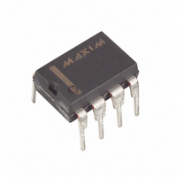
MAX8211CPA+ Maxim Integrated Products, MAX8211CPA+ Datasheet - Page 4

MAX8211CPA+
Manufacturer Part Number
MAX8211CPA+
Description
IC V-MONITOR W/PROG DETEC 8-DIP
Manufacturer
Maxim Integrated Products
Type
Simple Reset/Power-On Resetr
Datasheet
1.MAX8212CSA.pdf
(7 pages)
Specifications of MAX8211CPA+
Number Of Voltages Monitored
1
Output
Open Drain or Open Collector
Reset
Active Low
Voltage - Threshold
Adjustable/Selectable
Operating Temperature
0°C ~ 70°C
Mounting Type
Through Hole
Package / Case
8-DIP (0.300", 7.62mm)
Undervoltage Threshold
1.11 V
Overvoltage Threshold
1.19 V
Manual Reset
No
Watchdog
No
Battery Backup Switching
Yes
Supply Voltage (max)
16.5 V
Supply Voltage (min)
2 V
Supply Current (typ)
15 uA
Maximum Power Dissipation
727 mW
Mounting Style
Through Hole
Maximum Operating Temperature
+ 70 C
Chip Enable Signals
No
Minimum Operating Temperature
0 C
Output Type
Active Low or Open Drain
Power Fail Detection
Yes
Lead Free Status / RoHS Status
Lead free / RoHS Compliant
Microprocessor Voltage Monitors
with Programmable Voltage Detection
Figure 2. MAX8212 Block Diagram
in the networks that set up the trip voltage, since the
comparator input (THRESH pin) is a low-leakage
MOSFET transistor. This further reduces system current
drain. The tolerance of the internal reference has also
been significantly improved, allowing for more precise
voltage detection without the use of potentiometers.
The available current from the HYST output has been
increased from 21µA to 10mA, making the hysteresis
feature easier to use. The disparity between the HYST
output and the voltage required at THRESH to switch
the OUT pin has also been reduced in the MAX8211
from 8mV to 0.1mV to eliminate output “chatter” or
oscillation.
Most voltage detection circuits operate with supplies of
15V or less; in these applications, the MAX8211/
MAX8212 will replace ICL8211/ICL8212s with the per-
formance advantages described above. However, note
that the CMOS parts have an absolute maximum sup-
ply-voltage rating of 18V, and should never be used in
applications where this rating could be exceeded.
Exercise caution when replacing ICL8211/ICL8212s in
closed-loop applications such as programmable
zeners. Although neither the ICL8211/ICL8212 nor the
MAX8211/MAX8212 are internally compensated, the
CMOS parts have higher gain and may not be stable
for the external compensation-capacitor values used in
lower-gain ICL8211/ICL8212 circuits.
4
________________________________________________________________________________________
THRESH
REFERENCE
1.15V
V+
P
N
HYST
OUT
Figure 3 shows the basic circuit for both undervoltage
detection (MAX8211) and overvoltage detection
(MAX8212). For applications where no hysteresis is
needed, R3 should be omitted. The ratio of R1 to R2 is
then chosen such that, for the desired trip voltage at V
1.15V is applied to the THRESH pin. Since the com-
parator inputs are very low-leakage MOSFET transis-
tors, the MAX8211/MAX8212 can use much higher
resistors values in the attenuator network than can the
bipolar ICL8211/ICL8212. See Table 1 for switching
delays.
Table 1. Switching Delays
To ensure noise-free output switching, hysteresis is
frequently used in voltage detectors. For both the
MAX8211 and MAX8212 the HYST output is on for
threshold voltages greater than 1.15V. R3 (Figure 3)
controls the amount of current (positive feedback) sup-
plied from the HYST output to the mid-point of the resis-
tor divider, and hence the magnitude of the hysteresis,
or dead-band.
Figure 3. Basic Overvoltage/Undervoltage Circuit
__________Applications Information
TYPICAL DELAYS
t
t
R2
R1
(on)
(off)
V
Voltage Detectors with Hysteresis
IN
R3
HYST
THRESH
MAX8211
Basic Voltage Detectors
1.5ms
MAX8211
MAX8212
40µs
V+
V+
GND
OUT
MAX8212
V
OUT
250µs
3ms
IN
,


