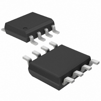
MAX706PCSA+ Maxim Integrated Products, MAX706PCSA+ Datasheet - Page 8

MAX706PCSA+
Manufacturer Part Number
MAX706PCSA+
Description
IC MPU SUPERVISORY CIRCUIT 8SOIC
Manufacturer
Maxim Integrated Products
Type
Simple Reset/Power-On Resetr
Datasheet
1.MAX708SCSA.pdf
(15 pages)
Specifications of MAX706PCSA+
Number Of Voltages Monitored
1
Output
Push-Pull, Totem Pole
Reset
Active High
Reset Timeout
140 ms Minimum
Voltage - Threshold
2.63V
Operating Temperature
0°C ~ 70°C
Mounting Type
Surface Mount
Package / Case
8-SOIC (3.9mm Width)
Monitored Voltage
2.63 V
Undervoltage Threshold
2.55 V
Overvoltage Threshold
2.7 V
Manual Reset
Resettable
Watchdog
Yes
Battery Backup Switching
No
Power-up Reset Delay (typ)
280 ms
Supply Voltage (max)
5.5 V
Supply Voltage (min)
1 V
Supply Current (typ)
350 uA
Maximum Power Dissipation
470.6 mW
Mounting Style
SMD/SMT
Maximum Operating Temperature
+ 70 C
Chip Enable Signals
No
Minimum Operating Temperature
0 C
Output Type
Active High or Push-Pull
Power Fail Detection
Yes
Lead Free Status / RoHS Status
Lead free / RoHS Compliant
WDO can be connected to the nonmaskable interrupt
(NMI) input of a µP. When V
threshold, WDO immediately goes low, even if the
watchdog timer has not timed out (Figure 3). Normally,
this would trigger an NMI, but since reset is asserted
simultaneously, the NMI is overridden. The WDO
should not be connected to RESET directly. Instead,
connect WDO to MR to generate a reset pulse when it
times out.
The manual reset (MR) input allows RESET and RESET
to be activated by a pushbutton switch. The switch is
effectively debounced by the 140ms minimum reset
pulse width. MR can be driven by an external logic line
since it is TTL/CMOS compatible. The minimum MR
+3V Voltage Monitoring, Low-Cost µP
Supervisory Circuits
Figure 3. RESET, RESET, MR, and WDO Timing
Figure 4. MAX706AP/AR/AS/AT Watchdog Timing
8
RESET
RESET
RESET
+3V/+3.3V
+3V/+3.3V
+3V/+3.3V
WDO*
WDO
WDI
MR*
V
CC
_______________________________________________________________________________________
+3.3V
+3.3V
+3.3V
+3.3V
+1V
0V
0V
0V
0V
0V
0V
0V
t
WP
V
RST
t
WD
V
RST
RESET EXTERNALLY
TRIGGERED BY MR
*NOTE: MR EXTERNALLY DRIVEN LOW.
t
RST
WDO TIMING SHOWN FOR MAX706P/R/S/T.
CC
t
WD
drops below the reset
t
MD
Manual Reset
t
MR
t
RST
t
RST
t
WD
input pulse width is 500ns when V
when V
to V
The power-fail comparator can be used for various pur-
poses because its output and noninverting input are
not internally connected. The inverting input is internally
connected to a 1.25V reference. The power-fail com-
parator has 10mV of hysteresis, which prevents repeat-
ed triggering of the power-fail output (PFO).
Figure 5. Monitoring Both +3V/+3.3V and +12V
Figure 6. RESET Valid to GND Circuit
CC
130kΩ
1MΩ
when not used.
CC
1%
1%
( ) ARE FOR MAX706P/AP
+12V RESET
THRESHOLD AT +25°C
+12V
= +5V. Leave MR unconnected or connect
PARAMETER
MAX706AR/AS/AT
+3V/+3.3V
MAX706R/S/T
MAX708R/S/T
RESET
V
PFI
CC
MAX708R/S/T
Power-Fail Comparator
10.24
MIN
MAX706_
GND
10.87
(RESET)
TYP
RESET
PFO
MR
CC
R1
11.50
MAX
= +3V and 150ns
UNIT
V
TO µP


