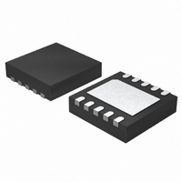
LTC2900-1CDD Linear Technology, LTC2900-1CDD Datasheet - Page 7

LTC2900-1CDD
Manufacturer Part Number
LTC2900-1CDD
Description
IC MON SUPP QUAD OPEN DRN 10DFN
Manufacturer
Linear Technology
Type
Multi-Voltage Supervisorr
Datasheet
1.LTC2900-2CMSPBF.pdf
(16 pages)
Specifications of LTC2900-1CDD
Number Of Voltages Monitored
4
Output
Open Drain or Open Collector
Reset
Active Low
Reset Timeout
5 ms Minimum
Voltage - Threshold
16 Selectable Threshold Combinations
Operating Temperature
0°C ~ 70°C
Mounting Type
Surface Mount
Package / Case
10-WFDFN Exposed Pad
Lead Free Status / RoHS Status
Contains lead / RoHS non-compliant
Available stocks
Company
Part Number
Manufacturer
Quantity
Price
Company:
Part Number:
LTC2900-1CDD
Manufacturer:
LT
Quantity:
10 000
Part Number:
LTC2900-1CDD#PBF
Manufacturer:
LINEAR/凌特
Quantity:
20 000
Company:
Part Number:
LTC2900-1CDD#TRPBF
Manufacturer:
LT
Quantity:
658
Part Number:
LTC2900-1CDD#TRPBF
Manufacturer:
LINEAR/凌特
Quantity:
20 000
PI FU CTIO S
V3 (Pin 1): Voltage Input 3. Select from 2.5V, 1.8V, 1.5V
or ADJ. See Table 1 for details.
V1 (Pin 2): Voltage Input 1. Select from 5V or 3.3V. See
Table 1 for details. The greater of (V1, V2) is also V
the device. Bypass this pin to ground with a 0.1 F (or
greater) capacitor.
CRT (Pin 3): Reset Delay Time Programming Pin. Attach
an external capacitor (C
of 4.6ms/nF. Leaving the pin open generates a minimum
delay of approximately 50 s. A 47nF capacitor will gener-
ate a 216ms reset delay time.
RST (Pin 4): Reset Logic Output. Active low with weak
pull-up to V2 (LTC2900-1) or active pull-up to V2
(LTC2900-2). Pulls low when any voltage input is below
the reset threshold and held low for the programmed delay
time after all voltage inputs are above threshold. May be
pulled above V2 using an external pull-up (LTC2900-1
only).
PBR (Pin 5): Manual Reset Pin. Attach a push-button
switch between this pin and ground. A logic low on this pin
will pull RST low. When the PBR pin returns high, RST will
return high after the programmed reset delay assuming all
four voltage inputs are above threshold. A weak internal
pull-up allows the pin to be left floating for normal monitor
U
U
U
RT
) to GND to set a reset delay time
CC
for
operation. When using a switch, the switch is debounced
through the reset circuitry using the delay provided by the
C
GND (Pin 6): Ground.
V
Connect to an external 1% resistive divider between V
and GND to select 1 of 16 combinations of preset and/or
capacitance on the V
V
nominal reference used for the programming voltage
(V
tions. The buffered reference can source and sink up to
1mA. The reference can drive a bypass capacitor of up to
1000pF without oscillation.
V4 (Pin 9): Voltage Input 4. Select from 1.8V, 1.5V, ADJ or
– ADJ. See Table 1 for details.
V2 (Pin 10): Voltage Input 2. Select from 3.3V, 3V or 2.5V.
See Table 1 for details. The greater of (V1, V2) is also V
for the device. Bypass this pin to ground with a 0.1 F (or
greater) capacitor. RST is weakly pulled up to V2
(LTC2900-1). RST is actively pulled up to V2 in the
LTC2900-2.
RT
PG
REF
adjustable voltage thresholds (see Table 1). Do not add
PG
timing capacitor.
(Pin 7): Voltage Threshold Combination Select Input.
) and for the offset of negative adjustable applica-
(Pin 8): Buffered Reference Voltage. A 1.210V
PG
pin.
LTC2900
7
2900f
REF
CC


