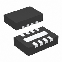
LTC2912CDDB-2#TRMPBF Linear Technology, LTC2912CDDB-2#TRMPBF Datasheet - Page 8

LTC2912CDDB-2#TRMPBF
Manufacturer Part Number
LTC2912CDDB-2#TRMPBF
Description
IC VOLT MONITOR SNGL 8-DFN
Manufacturer
Linear Technology
Type
Simple Reset/Power-On Resetr
Datasheet
1.LTC2912CTS8-1TRMPBF.pdf
(12 pages)
Specifications of LTC2912CDDB-2#TRMPBF
Number Of Voltages Monitored
1
Output
Open Drain or Open Collector
Reset
Active High/Active Low
Reset Timeout
Adjustable/Selectable
Voltage - Threshold
Adjustable/Selectable
Operating Temperature
0°C ~ 70°C
Mounting Type
Surface Mount
Package / Case
8-DFN
Lead Free Status / RoHS Status
Lead free / RoHS Compliant
Other names
LTC2912CDDB-2#TRMPBFTR
Available stocks
Company
Part Number
Manufacturer
Quantity
Price
APPLICATIONS INFORMATION
LTC2912
Power-Up/Power-Down
As soon as V
asserts low and the OV output weakly pulls to V
The LTC2912 is guaranteed to assert UV low, OV high
(LTC2912-1, LTC2912-2) and OV low (LTC2912-3) under
conditions of low V
(2.1V maximum), the VH and VL inputs take control.
Once the VH input and V
is started. After an adjustable delay time, UV weakly pulls
high.
Threshold Accuracy
Reset threshold accuracy is important in a supply-sensitive
system. Ideally, such a system resets only if supply voltages
fall outside the exact thresholds for a specifi ed margin.
Both LTC2912 inputs have a relative threshold accuracy
of ±1.5% over the full operating temperature range.
For example, when the LTC2912 is programmed to moni-
tor a 5V input with a 10% tolerance, the desired UV trip
point is 4.5V. Because of the ±1.5% relative accuracy of
the LTC2912, the UV trip point can be anywhere between
4.433V and 4.567V which is 4.5V ±1.5%.
Likewise, the accuracy of the resistances chosen for R
R
Using the example just given, if the resistances used to
set the UV trip point have 1% accuracy, the UV trip range
is between 4.354V and 4.650V. This is illustrated in the
following calculations.
The UV trip point is given as:
8
B
V
and R
UV
= 0.5V 1+
C
can affect the UV and OV trip points as well.
CC
reaches 1V during power up, the UV output
CC
R
, down to V
A
R
+ R
CC
C
become valid an internal timer
B
CC
= 1V. Above V
CC
CC
.
= 2V
A
,
The two extreme conditions, with a relative accuracy of
1.5% and resistance accuracy of 1%, result in:
Therefore,
Glitch Immunity
In any supervisory application, noise riding on the moni-
tored DC voltage causes spurious resets. To solve this
problem without adding hysteresis, which causes a new
error term in the trip voltage, the LTC2912 lowpass fi lters
the output of the fi rst stage comparator at each input. This
fi lter integrates the output of the comparator before as-
serting the UV or OV logic. A transient at the input of the
comparator of suffi cient magnitude and duration triggers
the output logic. The Typical Performance Characteristics
show a graph of the Transient Duration vs Comparator
Overdrive.
UV/OV Timing
The LTC2912 has an adjustable timeout period (t
holds OV, OV or UV asserted after each fault has cleared.
This delay assures a minimum reset pulse width allowing
settling time for the monitored voltage after it has entered
the “valid” region of operation.
For a desired trip point of 4.5V,
and
and
V
V
V
V
UV(MIN)
UV(MAX)
UV(MIN)
UV(MAX)
= 0.5V • 0.985 • 1+
= 0.5V • 0.985 • 1+ 8 0.99
= 0.5V • 1.015 • 1+
= 0.5V • 1.015 • 1+ 8 1.01
(
R
(
R
R
1.01
A
0.99
A
A
R
R
+ R
R
+ R
C
C
+ R
C
• 0.99
B
B
• 1.01
B
= 4.354V
= 4.650V
)
= 8
)
• 1.01
• 0.99
UOTO
) that
2912fa


