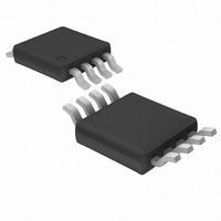
LTC1727EMS8-5 Linear Technology, LTC1727EMS8-5 Datasheet - Page 7

LTC1727EMS8-5
Manufacturer Part Number
LTC1727EMS8-5
Description
IC MON TRPL SPPLY MICROPWR 8MSOP
Manufacturer
Linear Technology
Type
Multi-Voltage Supervisorr
Datasheet
1.LTC1727EMS8-2.5PBF.pdf
(16 pages)
Specifications of LTC1727EMS8-5
Number Of Voltages Monitored
3
Output
Open Drain or Open Collector
Reset
Active Low
Reset Timeout
140 ms Minimum
Voltage - Threshold
3.086V, 4.675V, Adj
Operating Temperature
-40°C ~ 85°C
Mounting Type
Surface Mount
Package / Case
8-MSOP, Micro8™, 8-uMAX, 8-uSOP,
Lead Free Status / RoHS Status
Contains lead / RoHS non-compliant
Available stocks
Company
Part Number
Manufacturer
Quantity
Price
Company:
Part Number:
LTC1727EMS8-5
Manufacturer:
LT
Quantity:
10 000
Part Number:
LTC1727EMS8-5
Manufacturer:
LINEAR/凌特
Quantity:
20 000
Company:
Part Number:
LTC1727EMS8-5#PBF
Manufacturer:
ROHM
Quantity:
10
Company:
Part Number:
LTC1727EMS8-5#PBF
Manufacturer:
LINEAR40
Quantity:
1 172
Part Number:
LTC1727EMS8-5#TRPBF
Manufacturer:
LT/凌特
Quantity:
20 000
Company:
Part Number:
LTC1727EMS8-5.0
Manufacturer:
LT
Quantity:
550
pin FuncTions
V
Pin. (3V Sense Input and Power Supply Pin for LTC1728-
1.8.) This pin provides power to the part when the voltage
on V
Bypass to ground with a ≥ 0.1µF ceramic capacitor.
V
This pin is used on the LTC1727-5/LTC1728-5 to provide
power to the part when the voltage on V
than the voltage on V
ceramic capacitor.
V
Pin. This pin is used on the LTC1727-2.5/LTC1728-2.5 to
provide power to the part when the voltage on V
greater than the voltage on V
a ≥0.1µF ceramic capacitor.
V
Pin. This pin is used on the LTC1728-1.8/LTC1728-3.3 to
provide power to the part when the voltage on V
greater than the voltage on V
a ≥0.1µF ceramic capacitor.
V
used, it can be tied to either V
GND (Pin 4/Pin 2): Ground.
CC3
CC5
CC25
CC18
CCA
CC3
(Pin 3/Pin 3): 1V Sense, High Impedance Input. If un-
(Pin 1/Pin 5): 3.3V Sense Input and Power Supply
(Pin 2/Pin 4): 5V Sense Input and Power Supply Pin.
(Pin 2/Pin 4): 2.5V Sense Input and Power Supply
(Pin 2/Pin 4): 1.8V Sense Input and Power Supply
is greater than the voltage on V
CC3
. Bypass to ground with a ≥0.1µF
(LTC1727/LTC1728)
CC3
CC3
CC3
. Bypass to ground with
. Bypass to ground with
or V
CC5
CC5
/V
CC5
/V
CC25
CC25
is greater
/V
/V
CC25
CC18
CC18
CC18
.
is
is
.
COMPA (Pin 5): V
Active high, open-drain logic output with weak pull-up to
V
V
pins are too low to power the internal bandgap reference
(typically < 2.0V). Can be pulled greater than V
an external pull-up.
RST (Pin 6/Pin 1): Reset Logic Output. Active low, open-
drain logic output with weak pull-up to V
up greater than V
when one or all of the supplies are below trip thresholds
and held for 200ms after all supplies become valid.
COMP5 (Pin 7): V
LTC1727-5. Active high, open-drain logic output with weak
pull-up to V
be pulled greater than V
COMP25 (Pin 7): V
LTC1727-2.5. Active high, open-drain logic output with
weak pull-up to V
V
pull-up.
COMP3 (Pin 8): V
Active high, open-drain logic output with weak pull-up to
V
greater than V
CC3
CCA
RT25
CC3
. Asserted when V
. Asserted when V
is below V
. Can be pulled greater than V
CC3
CC3
. Asserted when V
RTA
CC3
CCA
CC3
using an external pull-up.
CC3
when interfacing to 5V logic. Asserted
LTC1727/LTC1728
or if both the V
Comparator Output for the LTC1727.
Comparator Output for the LTC1727.
CC5
CC25
CCA
. Asserted when V
CC3
CC3
is above V
Comparator Output for the
Comparator Output for the
is above V
using an external pull-up.
CC5
RTA
CC3
CC3
is above V
RT3
. Deasserted when
CC3
using an external
and V
. Can be pulled
CC25
. Can be pulled
CC5
CC3
is above
RT5
supply
using
. Can
17278fb
7


