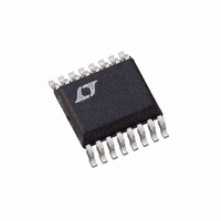
LTC2902-2CGN Linear Technology, LTC2902-2CGN Datasheet - Page 8

LTC2902-2CGN
Manufacturer Part Number
LTC2902-2CGN
Description
IC MON SUPP QD W/RST&SEL 16-SSOP
Manufacturer
Linear Technology
Type
Multi-Voltage Supervisorr
Datasheet
1.LTC2902-1CGNPBF.pdf
(16 pages)
Specifications of LTC2902-2CGN
Number Of Voltages Monitored
4
Output
Push-Pull, Totem Pole
Reset
Active Low
Reset Timeout
5 ms Minimum
Voltage - Threshold
16 Selectable Threshold Combinations
Operating Temperature
0°C ~ 70°C
Mounting Type
Surface Mount
Package / Case
16-SSOP
Lead Free Status / RoHS Status
Contains lead / RoHS non-compliant
Available stocks
Company
Part Number
Manufacturer
Quantity
Price
Company:
Part Number:
LTC2902-2CGN
Manufacturer:
LT
Quantity:
10 000
Part Number:
LTC2902-2CGN
Manufacturer:
LINEAR/凌特
Quantity:
20 000
Company:
Part Number:
LTC2902-2CGN#PBF
Manufacturer:
Linear Technology
Quantity:
135
LTC2902
PI FU CTIO S
RST (Pin 6): Reset Logic Output. Active low with weak
pull-up to V2 (LTC2902-1) or active pull-up to V2
(LTC2902-2). Pulls low when any voltage input is below
the reset threshold and held low for programmed delay
time after all voltage inputs are above threshold. May be
pulled above V2 using an external pull-up (LTC2902-1
only).
T0 (Pin 7): Digital Input for Supply Tolerance Selection
(5%, 7.5%, 10% or 12.5%). Used in conjunction with T1
(Pin 9). See Applications Information for tolerance selec-
tion chart (Table 4).
RDIS (Pin 8): Digital Input for RST Disable. A low input on
this pin forces the RST output to V2 (or pull-up voltage).
Useful for determining supply margins without issuing
reset command to processor. A weak internal pull-up
allows pin to be left floating for normal monitor operation.
T1 (Pin 9): Digital Input for Supply Tolerance Selection
(5%, 7.5%, 10% or 12.5%). Used in conjunction with T0
(Pin 7). See Applications Information for tolerance selec-
tion chart (Table 4).
GND (Pin 10): Ground.
V
Input. Connect to an external 1% resistive divider be-
tween V
preset and/or adjustable voltage thresholds (see Table 1).
Do not add capacitance on the V
8
PG
U
(Pin 11): Voltage Threshold Combination Select
REF
U
and GND to select 1 of 16 combinations of
U
PG
pin.
V
nominal reference used for programming voltage (V
and for the offset of negative adjustable applications. The
buffered reference can source and sink up to 1mA. The
reference can drive a bypass capacitor of up to 1000pF
without oscillation.
V4 (Pin 13): Voltage Input 4. Select from 1.8V, 1.5V, ADJ
or – ADJ. See Table 1 for details.
V2 (Pin 14): Voltage Input 2. Select from 3.3V, 3V or 2.5V.
See Table 1 for details. The greater of (V1, V2) is also V
for chip. Bypass this pin to ground with a 0.1 F (or greater)
capacitor. All logic outputs (COMP1, COMP2, COMP3,
COMP4) are weakly pulled up to V2. RST is weakly pulled
up to V2 in the LTC2902-1 and RST is actively pulled up to
V2 in the LTC2902-2.
COMP4 (Pin 15): Comparator Output 4. Nondelayed,
active high logic output with weak pull-up to V2. Pulls high
when V4 is above reset threshold. May be pulled greater
than V2 using external pull-up.
COMP2 (Pin 16): Comparator Output 2. Nondelayed,
active high logic output with weak pull-up to V2. Pulls high
when V2 is above reset threshold. May be pulled greater
than V2 using external pull-up.
REF
(Pin 12): Buffered Reference Voltage. A 1.210V
2902f
PG
CC
)


