BD4833FVE-TR Rohm Semiconductor, BD4833FVE-TR Datasheet - Page 5
BD4833FVE-TR
Manufacturer Part Number
BD4833FVE-TR
Description
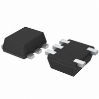
IC DETECTOR VOLT 3.3V ODRN 5VSOF
Manufacturer
Rohm Semiconductor
Type
Simple Reset/Power-On Resetr
Specifications of BD4833FVE-TR
Number Of Voltages Monitored
1
Output
Open Drain or Open Collector
Reset
Active Low
Voltage - Threshold
3.3V
Operating Temperature
-40°C ~ 105°C
Mounting Type
Surface Mount
Package / Case
5-VSOF
Lead Free Status / RoHS Status
Lead free / RoHS Compliant
Reset Timeout
-
Available stocks
Company
Part Number
Manufacturer
Quantity
Price
Company:

Part Number:
BD4833FVE-TR
Manufacturer:
SONY
Quantity:
1 654


Reference Data
Explanation of Operation
Timing Waveform
© 2009 ROHM Co., Ltd. All rights reserved.
BD48□□G, BD48□□FVE, BD49□□G, BD49□□FVE series
www.rohm.com
V
V
For both the open drain type (Fig.12) and the CMOS output type (Fig.13), the detection and release voltages are used as
threshold voltages. When the voltage applied to the VDD pins reaches the applicable threshold voltage, the VOUT terminal
voltage switches from either “High” to “Low” or from “Low” to “High”. Because the BD48□□G/FVE series uses an open drain
output type, it is possible to connect a pull-up resistor to VDD or another power supply [The output “High” voltage (VOUT) in
this case becomes VDD or the voltage of the other power supply].
DD
OUT
V
Examples of Leading (TPLH) and Falling (TPHL) Output
*This data is for reference only.
DET
Example: the following shows the relationship between the input voltages VDD and the output voltage VOUT when the
input power supply voltage VDD is made to sweep up and sweep down (the circuits are those in Fig.12 and 13).
0V
The figures will vary with the application, so please confirm actual operating conditions before use.
V
V
+ΔV
OH
OL
Fig.12 (BD48□□ Type Internal Block Diagram)
Vref
V
BD4845G/FVE
BD4945G/FVE
V
OPL
Part Number
DET
DET
T
PHL
①
R1
R2
R3
②
Fig.14
T
PLH
T
PHL
③
VDD=4.3V5.1V
④
Q1
TPLH (μs)
39.5
32.4
T
⑤
V
V
PLH
DD
OUT
GND
R
L
after over the operating limit voltage (VOPL) until TPHL. There fore it
is possible that the reset signal is not outputted when the rise time of
VDD is faster than TPHL.
voltage (VS + ∆VS), the output voltages will switch to Low.
VOUT switches from L to H.
supply is powered down or when there is a power supply fluctuation,
VOUT switches to L (with a delay of TPHL).
release voltage is known as the hysteresis width (∆VS). The system
is designed such that the output does not flip-flop with power supply
fluctuations within this hysteresis width, preventing malfunctions due
to noise.
1
2
3
4
5
5/9
When the power supply is turned on, the output is unsettled from
When VDD is greater than VOPL but less than the reset release
If VDD drops below the detection voltage (VS) when the power
The potential difference between the detection voltage and the
If VDD exceeds the reset release voltage (VS + ∆VS), then
VDD=5.1V4.3V
Vref
Fig.13 (BD49□□ Type Internal Block Diagram)
TPHL (μs)
87.8
52.4
R1
R2
R3
Technical Note
2009.04 - Rev.A
Q2
Q1
V
V
GND
DD
OUT
Related parts for BD4833FVE-TR
Image
Part Number
Description
Manufacturer
Datasheet
Request
R

Part Number:
Description:
Manufacturer:
Rohm Semiconductor
Datasheet:
Part Number:
Description:
Manufacturer:
Rohm Semiconductor
Datasheet:
Part Number:
Description:
Manufacturer:
Rohm Semiconductor
Datasheet:
Part Number:
Description:
Manufacturer:
Rohm Semiconductor
Datasheet:
Part Number:
Description:
Manufacturer:
Rohm Semiconductor
Datasheet:
Part Number:
Description:
Manufacturer:
Rohm Semiconductor
Datasheet:
Part Number:
Description:
Manufacturer:
Rohm Semiconductor
Datasheet:
Part Number:
Description:
Manufacturer:
Rohm Semiconductor
Datasheet:
Part Number:
Description:
Manufacturer:
Rohm Semiconductor
Datasheet:
Part Number:
Description:
Manufacturer:
Rohm Semiconductor
Datasheet:
Part Number:
Description:
Manufacturer:
Rohm Semiconductor
Datasheet:
Part Number:
Description:
Manufacturer:
Rohm Semiconductor
Datasheet:

Part Number:
Description:
DIODE SWITCH 80V 25MA SMD5 TR
Manufacturer:
Rohm Semiconductor
Datasheet: