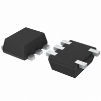
BU4216FVE-TR Rohm Semiconductor, BU4216FVE-TR Datasheet - Page 8

BU4216FVE-TR
Manufacturer Part Number
BU4216FVE-TR
Description
IC DETECTOR VOLT 1.6V ODRN 5VSOF
Manufacturer
Rohm Semiconductor
Type
Simple Reset/Power-On Resetr
Specifications of BU4216FVE-TR
Number Of Voltages Monitored
1
Output
Open Drain or Open Collector
Reset
Active Low
Reset Timeout
Adjustable/Selectable
Voltage - Threshold
1.6V
Operating Temperature
-40°C ~ 125°C
Mounting Type
Surface Mount
Package / Case
5-VSOF
Lead Free Status / RoHS Status
Lead free / RoHS Compliant
●Notes for use
© 2009 ROHM Co., Ltd. All rights reserved.
BU42□□G series, BU42□□F series, BU42□□FVE series,
BU43□□G series, BU43□□F series, BU43□□FVE series
www.rohm.com
10. Case of needless Delay time, recommended to insert more 470kΩ resister between V
12. This IC has extremely high impedance terminals. Small leak current due to the uncleanness of PCB surface might cause
1. Absolute maximum range
2 . GND potential
3 . Electrical Characteristics
4 . Bypass Capacitor for Noise Rejection
5 . Short Circuit between Terminal and Soldering
6 . Electromagnetic Field
7 . The V
8 . A V
9 . Lower than the mininum input voltage makes the V
Absolute Maximum Ratings are those values beyond which the life of a device may be destroyed. We cannot be defined the
failure mode, such as short mode or open mode. Therefore a physical security countermeasure, like fuse, is to be given
when a specific mode to be beyond absolute maximum ratings is considered.
Recommended value of RL Resistar is over 50kΩ (VDET=1.5~4.8V),over 100kΩ (VDET=0.9~1.4V).
unexpected operations. Application values in these conditions should be selected carefully. If 10MΩ leakage is assumed
between the CT terminal and the GND terminal, 1MΩ connection between the CT terminal and the V
recommended. Also, if the leakage is assumed between the V
should be less than 1/10 of the assumed leak resistance.
The value of R
that is decided by τ × RCT × CCT changes.
GND terminal should be a lowest voltage potential every state.
Please make sure all pins that are over ground even if include transient feature.
Be sure to check the electrical characteristics, that are one the tentative specification will be changed by temperature,
supply voltage, and external circuit.
Please put into the to reject noise between V
If extremely big capacitor is used, transient response might be late. Please confirm sufficiently for the point.
Don’t short-circuit between Output pin and V
IC on circuit board please is unusually cautious about the orientation and the position of the IC. When the orientation is
mistaken the IC may be destroyed.
Mal-function may happen when the device is used in the strong electromagnetic field.
DD
DD
-GND capacitor (as close connection as possible) should be used in high V
line inpedance might cause oscillation because of the detection current.
CT
depends on the external resistor that is connected to CT terminal, so please consider the delay time
DD
DD
pin, Output pin and GND pin, or V
pin and GND with 1uF over and between V
OUT
8/11
high impedance, and it must be V
OUT
terminal and the GND terminal, the pull up resistor
DD
DD
pin and GND pin. When soldering the
line impedance condition.
DD
and CT.
OUT
DD
in pull up (V
pin and GND with 1000pF.
DD
Technical Note
2009.11 - Rev.C
terminal would be
DD
) condition.


