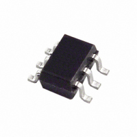
ADM1086AKSZ-REEL7 Analog Devices Inc, ADM1086AKSZ-REEL7 Datasheet

ADM1086AKSZ-REEL7
Specifications of ADM1086AKSZ-REEL7
ADM1086AKSZ-REEL7TR
Available stocks
Related parts for ADM1086AKSZ-REEL7
ADM1086AKSZ-REEL7 Summary of contents
Page 1
FEATURES Provide programmable time delays between enable signals Can be cascaded with power modules for multiple supply sequencing Power supply monitoring from 0.6 V Output stages High voltage ( open-drain output (ADM1085/ADM1087) Push-pull output (ADM1086/ADM1088) Capacitor-adjustable time ...
Page 2
ADM1085/ADM1086/ADM1087/ADM1088 TABLE OF CONTENTS Features .............................................................................................. 1 Applications....................................................................................... 1 Functional Block Diagrams............................................................. 1 General Description ......................................................................... 1 Revision History ............................................................................... 2 Specifications..................................................................................... 3 Absolute Maximum Ratings............................................................ 4 ESD Caution.................................................................................. 4 Pin Configuration and Function Descriptions............................. 5 Typical Performance Characteristics ............................................. ...
Page 3
SPECIFICATIONS V = full operating range −40°C to +125°C, unless otherwise noted Table 2. Parameter SUPPLY V Operating Voltage Range CC V Operating Voltage Range IN Supply Current V Rising Threshold TH_RISING V Falling ...
Page 4
ADM1085/ADM1086/ADM1087/ADM1088 ABSOLUTE MAXIMUM RATINGS T = 25°C, unless otherwise noted. A Table 3. Parameter CEXT ENIN, ENIN ENOUT, ENOUT (ADM1085, ADM1087) ENOUT, ENOUT (ADM1086, ADM1088) Operating Temperature Range Storage Temperature Range θ Thermal Impedance, SC70 JA ...
Page 5
PIN CONFIGURATION AND FUNCTION DESCRIPTIONS Table 4. Pin Function Descriptions Pin No. Mnemonic Description 1 ENIN, ENIN Enable Input. Controls the status of the enable output. Active high for ADM1085/ADM1086. Active low for ADM1087/ADM1088. 2 GND Ground Input ...
Page 6
ADM1085/ADM1086/ADM1087/ADM1088 TYPICAL PERFORMANCE CHARACTERISTICS 700 680 660 640 V RISING TRIP 620 600 580 560 V FALLING TRIP 540 520 500 –40 –25 – TEMPERATURE (°C) Figure 3. V Threshold vs. Temperature IN 12.0 11.5 ...
Page 7
SUPPLY VOLTAGE (V) Figure 9. Output Low Voltage vs. Supply Voltage 100 1mV/µ 10mV/µ –40 –25 – ...
Page 8
ADM1085/ADM1086/ADM1087/ADM1088 300 280 260 240 220 200 180 160 140 120 100 –40 –25 – TEMPERATURE (°C) Figure 15. CEXT Charge Current vs. Temperature 100 ...
Page 9
CIRCUIT INFORMATION TIMING CHARACTERISTICS AND TRUTH TABLES The enable outputs of the ADM1085/ADM1086/ADM1087/ ADM1088 are related to the V and enable inputs by a simple IN AND function. The enable output is asserted only if the enable input is asserted ...
Page 10
ADM1085/ADM1086/ADM1087/ADM1088 OPEN-DRAIN AND PUSH-PULL OUTPUTS The ADM1085 and ADM1087 have open-drain output stages that require an external pull-up resistor to provide a logic high voltage level. The geometry of the NMOS transistor enables the output to be pulled up to ...
Page 11
APPLICATION INFORMATION SEQUENCING CIRCUITS The ADM1085/ADM1086/ADM1087/ADM1088 are compatible with voltage regulators and dc-to-dc converters that have active high or active low enable or shutdown inputs, with a choice of open-drain or push-pull output stages. Figure 23 to Figure 25 illustrate ...
Page 12
ADM1085/ADM1086/ADM1087/ADM1088 12V IN EN OUT DC/DC 3.3V 3. ENOUT IN ADM1086 ENIN CEXT ENABLE CONTROL 12V 3.3V 2.5V 1.8V 1.2V 12V IN SD OUT ADP3334 3.3V 3. ENOUT IN ADM1087 ENIN CEXT Figure 25. ...
Page 13
DUAL LOFO SEQUENCING A power sequencing solution for a portable device, such as a PDA, is shown in Figure 27. This solution requires that the microprocessor power supply turn on before the LCD display turns on, and that the LCD ...
Page 14
ADM1085/ADM1086/ADM1087/ADM1088 QUAD-SUPPLY POWER GOOD INDICATOR The enable output of the Simple Sequencers is equivalent to an AND function of V and ENIN. ENOUT is high only when IN the voltage above the threshold and the enable input ...
Page 15
... Temperature Model Range ADM1085AKS-REEL7 −40°C to +125°C ADM1085AKSZ-REEL7 1 −40°C to +125°C ADM1086AKS-REEL7 −40°C to +125°C 1 ADM1086AKSZ-REEL7 −40°C to +125°C ADM1087AKS-REEL7 −40°C to +125°C ADM1087AKSZ-REEL7 1 −40°C to +125°C ADM1088AKS-REEL7 −40°C to +125°C 1 ADM1088AKSZ-REEL7 −40°C to +125°C ...
Page 16
ADM1085/ADM1086/ADM1087/ADM1088 NOTES ©2006 Analog Devices, Inc. All rights reserved. Trademarks and registered trademarks are the property of their respective owners. D04591-0-4/06(A) T Rev Page ...


