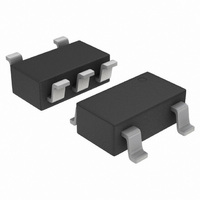
NCP303LSN20T1G ON Semiconductor, NCP303LSN20T1G Datasheet - Page 16

NCP303LSN20T1G
Manufacturer Part Number
NCP303LSN20T1G
Description
IC VOLT DETECT OD 2.0V SOT23-5
Manufacturer
ON Semiconductor
Type
Simple Reset/Power-On Resetr
Datasheet
1.NCP303LSN30T1G.pdf
(26 pages)
Specifications of NCP303LSN20T1G
Number Of Voltages Monitored
1
Output
Open Drain or Open Collector
Reset
Active Low
Reset Timeout
Adjustable/Selectable
Voltage - Threshold
2V
Operating Temperature
-40°C ~ 85°C
Mounting Type
Surface Mount
Package / Case
TSOT-23-5, TSOT-5, TSOP-5
Undervoltage Threshold
1.96 V
Overvoltage Threshold
2.04 V
Output Type
Open Collector / Drain
Supply Voltage (max)
10 V
Supply Voltage (min)
0.8 V
Supply Current (typ)
1.3 uA
Operating Temperature Range
- 40 C to + 125 C
Mounting Style
SMD/SMT
Manual Reset
No
Watchdog
No
Lead Free Status / RoHS Status
Lead free / RoHS Compliant
Available stocks
Company
Part Number
Manufacturer
Quantity
Price
Part Number:
NCP303LSN20T1G
Manufacturer:
ON/安森美
Quantity:
20 000
precision voltage detector that drives a time delay generator.
Figures 37 and 38 show a timing diagram and a typical
application. Initially consider that input voltage V
nominal level and it is greater than the voltage detector upper
threshold (V
will be at the same level as V
will be in the high state for active low devices, or in the low
state for active high devices. If there is a power interruption
and V
lower detector threshold (V
delay capacitor C
internal N−Channel MOSFET that connects to Pin 5. This
sequence of events causes the Reset output to be in the low
state for active low devices, or in the high state for active
high devices. After completion of the power interruption,
The NCP302 and NCP303 series devices consist of a
in
becomes significantly deficient, it will fall below the
Reset Output (Active High), Pin 1
Reset Output (Active Low), Pin 1
DET+
OPERATING DESCRIPTION
). The voltage at Pin 5 and capacitor C
D
will be immediately discharged by an
Input Voltage, Pin 2
Capacitor, Pin 5
in
DET−
, and the reset output (Pin 1)
) and the external time
0.675 V
Figure 37. Timing Waveforms
V
V
V
V
DET
DET−
DET−
DET−
0 V
0 V
V
V
V
V
in
in
in
in
in
in
+
http://onsemi.com
is at a
D
16
V
than the V
N−Channel MOSFET and allow pullup resistor R
external capacitor C
for releasing the reset signal. When the voltage at Pin 5
exceeds the inverter/buffer threshold, typically 0.675 V
the reset output will revert back to its original state. The reset
output time delay versus capacitance is shown in Figures 30
through 32. The voltage detector and inverter/buffer have
built−in hysteresis to prevent erratic reset operation.
use as reset controllers in portable microprocessor based
systems, they offer a cost−effective solution in numerous
applications where precise voltage monitoring and time
delay are required. Figures 38 through 46 show various
application examples.
in
Although these device series are specifically designed for
will again return to its nominal level and become greater
DET+
t
D2
. The voltage detector will turn off the
D
, thus creating a programmable delay
D
to charge
in
,


