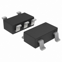
NCP301LSN11T1G ON Semiconductor, NCP301LSN11T1G Datasheet - Page 16

NCP301LSN11T1G
Manufacturer Part Number
NCP301LSN11T1G
Description
IC VOLTAGE DETECTOR 1.1V SOT23-5
Manufacturer
ON Semiconductor
Type
Simple Reset/Power-On Resetr
Datasheet
1.NCP300HSN47T1G.pdf
(26 pages)
Specifications of NCP301LSN11T1G
Number Of Voltages Monitored
1
Output
Open Drain or Open Collector
Reset
Active Low
Voltage - Threshold
1.1V
Operating Temperature
-40°C ~ 85°C
Mounting Type
Surface Mount
Package / Case
TSOT-23-5, TSOT-5, TSOP-5
Mounting Style
SMD/SMT
Lead Free Status / RoHS Status
Lead free / RoHS Compliant
Reset Timeout
-
Available stocks
Company
Part Number
Manufacturer
Quantity
Price
Company:
Part Number:
NCP301LSN11T1G
Manufacturer:
ON Semiconductor
Quantity:
2 100
So, V
variable V
For example, for NCP300LSN18T1G V
then
The NCP30X detection voltage option must be chosen such
that:
sure the the reset from NCP30X remains asserted (in RESET
hold state) till after the power supply exceeds the V
requirement; this prevents incorrect device (uP) initiation.
NCP30X is able to start up when V
selected by the user, V
following formula:
The following example shows how to select the device
voltage option in a real world application.
So, we have:
Then the ideal voltage option = (3.201 + 3.135) / (2 * 1.09)
= 2.9064 V
Therefore, a device voltage option of 2.9 V will be the right
choice.
The significance of V
Having V
The theoretical ideal V
1. Power supply output specification: 3.3 V $3%
2. Microprocessor core voltage specification: 3.3 V
DET+_max
$5%
V
DET−_typ
V
DET−_typ_ideal
V
DET+_max
DET+_max
V
V
CC_min
in_min
CC_min
can be easily figured out just using a single
.
+ 3.3 V * 3% + 3.201 V
+ 3.3 V * 5% + 3.135 V
+ 1.8
t V
CC_min
DET−_typ_ideal
+
< V
DET+_max
DET−_typ
V
in_min
in_min
< V
1.09 + 1.962 V
( 2
DET+_max
in
) V
t V
makes sure that the
voltage option to be
, can be given by the
1.09 )
is at the V
CC_min
in_min
DET−_typ
is that it makes
in_min
= 1.8 V;
(eq. 10)
(eq. 12)
(eq. 11)
(eq. 8)
(eq. 9)
CC_min
http://onsemi.com
.
16
overdrive value from V
That means V
enough than V
significantly increasing propagation delay. (Figure 25) This
propagation delay is temperature sensitive.
difference between V
On the other hand (see above paragraph), a minimum
To avoid acceptable time response, a minimum 100 mV
600
500
400
300
200
100
3.0
0
V
Figure 25. t
DET
3.168
PROPAGATION DELAY VARIATION
+
in
V
in
DET+
(minimum value of V
, PULSE HIGH INPUT VOLTAGE (V)
3.5
for the NCP301SNT1
pLH
t
pHL
in
(V
and t
and V
t
threshold
pLH
DET−
4.0
pHL
DET+
+ hysteresis) at the risk of
to V
vs. Input Voltage
must be selected.
CC
4.5
CC
must be respected.
) must be higher
5.0
5.5


