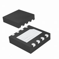
MAX6769TAYD2+T Maxim Integrated Products, MAX6769TAYD2+T Datasheet - Page 17

MAX6769TAYD2+T
Manufacturer Part Number
MAX6769TAYD2+T
Description
IC REG LINEAR 2.5V/ADJ 8-TDFN
Manufacturer
Maxim Integrated Products
Type
Regulator/Supervisorr
Datasheet
1.MAX6765TTSD2T.pdf
(22 pages)
Specifications of MAX6769TAYD2+T
Number Of Voltages Monitored
1
Output
Open Drain or Open Collector
Reset
Active Low
Reset Timeout
8.75 ms Minimum
Voltage - Threshold
2.188V
Operating Temperature
-40°C ~ 125°C
Mounting Type
Surface Mount
Package / Case
8-TDFN Exposed Pad
Lead Free Status / RoHS Status
Lead free / RoHS Compliant
The MAX6765–MAX6774B provide up to 100mA of load
current. Package power dissipation limits the amount of
output current available for a given input/output voltage
and ambient temperature. Figures 3 and 4 depict the
maximum power dissipation curve for the MAX6765/
MAX6766 and MAX6767–MAX6774B, respectively. The
graph assumes that the exposed metal pad of the
device package is soldered to a solid 1in
2oz. PCB copper (JESD51-3 AND JESD51-5). Use
Figure 4 to determine the allowable package dissipa-
tion for a given ambient temperature. Alternately, use
the following formula to calculate the allowable pack-
age dissipation:
PD
where 0.0244W is the MAX6767–MAX6774B package
thermal derating in W/°C and T
ture in °C, under the same conditions used for Figure 4.
After determining the allowable package dissipation,
calculate the maximum output current using the follow-
ing formula:
Also, I
Figure 3. Maximum Power Dissipation vs. Temperature
(MAX6765/MAX6766)
MAX
PD
PD < PD
MAX
OUT
= Max. Power Dissip = 1.951W, for T
Available Output-Current Calculation
= Max. Power Dissip = [1.9W - 0.0244W x
should be ≤ 100mA in any case.
1.8
1.6
1.4
1.2
1.0
0.6
2.2
2.0
0.8
0.4
0.2
(T
0
Automotive Micropower Linear Regulators
MAX
0
A
- 70°C)], for +70°C < T
1.904W
where PD = [(V
20
______________________________________________________________________________________
SAFE OPERATING
AREA
40
TEMPERATURE (°C)
60
80
A
DERATE 23.8mW/°C
ABOVE +70°C
is the ambient tempera-
100
IN
- V
120
OUT
A
140
≤ +125°C
) x I
2
160
A
section of
≤ +70°C
OUT
]
The reset timeout period is adjustable to accommodate
a variety of µP applications. Adjust the reset timeout
period by connecting a capacitor between TIMEOUT
and GND.
where t
Connect TIMEOUT to OUT to select the internally fixed
timeout period. C
(< 10nA) type capacitor. Ceramic capacitors are
recommended; do not use capacitor values lower than
100pF to avoid the influence of parasitic capacitances.
For stable operation over the full temperature range and
with load currents up to 100mA, use a 10µF (min) output
capacitor with an ESR < 0.5Ω. To reduce noise and
improve load-transient response, stability, and power-
supply rejection, use larger output-capacitor values.
Some ceramic dielectrics exhibit large capacitance
and ESR variation with temperature. For dielectric
capacitors such as Z5U and Y5V, use more capaci-
tance to ensure stability at low temperatures. With X7R
or X5R dielectrics, 10µF should be sufficient at all oper-
ating temperatures. For higher-ESR tantalum capaci-
tors, use larger capacitor values to maintain stability. To
improve power-supply rejection and transient
response, use a larger capacitor than the minimum
0.1µF capacitor between IN and GND.
Figure 4. Maximum Power Dissipation vs. Temperature
(MAX6767–MAX6774B)
RP
is in seconds and C
2.2
2.0
1.8
1.6
1.4
1.2
1.0
0.8
0.6
0.4
0.2
0
t
RP
0
= C
1.951W
SAFE OPERATING
AREA
with Supervisor
20
Selecting Timeout Capacitor
TIMEOUT
TIMEOUT
40
TEMPERATURE (°C)
Capacitor Selection and
60
80
x 1.22 x 10
must be a low-leakage
TIMEOUT
DERATE 24.4mW/°C
ABOVE +70°C
Regulator Stability
100
120
is in Farads.
140
6
Ω
160
17


