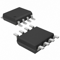
MAX795RCSA+T Maxim Integrated Products, MAX795RCSA+T Datasheet - Page 12

MAX795RCSA+T
Manufacturer Part Number
MAX795RCSA+T
Description
IC SUPERVISOR MPU 8-SOIC
Manufacturer
Maxim Integrated Products
Type
Battery Backup Circuitr
Datasheet
1.MAX795TCSA.pdf
(20 pages)
Specifications of MAX795RCSA+T
Number Of Voltages Monitored
1
Output
Open Drain or Open Collector
Reset
Active Low
Reset Timeout
140 ms Minimum
Voltage - Threshold
2.625V
Operating Temperature
0°C ~ 70°C
Mounting Type
Surface Mount
Package / Case
8-SOIC (3.9mm Width)
Monitored Voltage
3 V, 3.3 V
Output Type
Active Low, Open Drain
Manual Reset
Not Resettable
Watchdog
No Watchdog
Battery Backup Switching
Backup
Supply Voltage (max)
5.5 V
Supply Voltage (min)
1 V
Supply Current (typ)
49 uA
Maximum Power Dissipation
471 mW
Maximum Operating Temperature
+ 70 C
Mounting Style
SMD/SMT
Minimum Operating Temperature
0 C
Power Fail Detection
No
Lead Free Status / RoHS Status
Lead free / RoHS Compliant
The CE transmission gate remains disabled and CE IN
remains high impedance (regardless of CE IN activity)
for the first half of the reset timeout period (t
time a reset is generated. While disabled, CE IN is high
impedance. When the CE transmission gate is enabled,
the impedance of CE IN appears as a 46Ω resistor in
series with the load at CE OUT.
3.0V/3.3V Adjustable Microprocessor
Supervisory Circuits
Figure 7. Chip-Enable Transmission Gate
Figure 8. Chip-Enable Timing
12
CE IN
V
RESET PULLED UP TO V
V
CE OUT
RESET
(PULLED TO V
CE IN
______________________________________________________________________________________
BATT
CC
= 3.6V
CHIP-ENABLE
GENERATOR
V
MAX793
MAX794
MAX795
CONTROL
BATT
OUTPUT
RESET
CC
)
t
V
RP
RST
/
CC
2
t
RP
P
N
OUT
RP
P
/ 2), any
CE OUT
V
RST
V
10µs
SW
V
BATT
The propagation delay through the CE transmission
gate depends on V
drive connected to CE IN, and the loading on CE OUT.
The CE propagation delay is production tested from the
50% point on CE IN to the 50% point on CE OUT using
a 50Ω driver and 50pF of load capacitance (Figure 9).
For minimum propagation delay, minimize the capaci-
tive load at CE OUT and use a low-output-impedance
driver.
When the CE transmission gate is enabled, the imped-
ance of CE OUT is equivalent to a 46Ω resistor in series
with the source driving CE IN. In the disabled mode,
the transmission gate is off and an active pullup con-
nects CE OUT to OUT (Figure 8). This pullup turns off
when the transmission gate is enabled.
Critical systems often require an early warning indicat-
ing that power is failing. This warning provides time for
the µP to store vital data and take care of any additional
“housekeeping” functions, before the power supply
gets too far out of tolerance for the µP to operate reli-
ably. The MAX793/MAX794 offer two methods of
achieving this early warning. If access to the unregulat-
ed supply is feasible, the power-fail comparator input
(PFI) can be connected to the unregulated supply
through a voltage divider, with the power-fail compara-
tor output (PFO) providing the NMI to the µP (Figure
V
RST
V
CC
CC
Early Power-Fail Warning
, the source impedance of the
(MAX793/MAX794)
Chip-Enable Output
V
RST
V
SW


