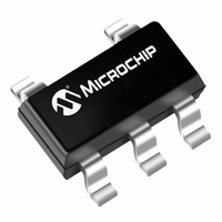
TC1185-3.0VCT713 Microchip Technology, TC1185-3.0VCT713 Datasheet - Page 3

TC1185-3.0VCT713
Manufacturer Part Number
TC1185-3.0VCT713
Description
IC CMOS LDO 3.0V 150MA SOT23A-5
Manufacturer
Microchip Technology
Specifications of TC1185-3.0VCT713
Package / Case
SOT-23-5, SC-74A, SOT-25
Regulator Topology
Positive Fixed
Voltage - Output
3V
Voltage - Input
Up to 6V
Voltage - Dropout (typical)
0.27V @ 150mA
Number Of Regulators
1
Current - Output
150mA (Min)
Operating Temperature
-40°C ~ 125°C
Mounting Type
Surface Mount
Number Of Outputs
1
Polarity
Positive
Input Voltage Max
6 V
Output Voltage
3 V
Output Type
Fixed
Dropout Voltage (max)
400 mV
Output Current
150 mA
Line Regulation
0.05 %
Load Regulation
0.5 %
Voltage Regulation Accuracy
2.5 %
Maximum Operating Temperature
+ 125 C
Mounting Style
SMD/SMT
Minimum Operating Temperature
- 40 C
Lead Free Status / RoHS Status
Lead free / RoHS Compliant
Current - Limit (min)
-
Lead Free Status / Rohs Status
Lead free / RoHS Compliant
Other names
TC1185-3.0VCT713
TC11853.0VCT713
TC11853.0VCT713RTR
TC11853.0VCT713RTR
TC11853.0VCT713TR
TC11853.0VCT713
TC11853.0VCT713RTR
TC11853.0VCT713RTR
TC11853.0VCT713TR
Available stocks
Company
Part Number
Manufacturer
Quantity
Price
Company:
Part Number:
TC1185-3.0VCT713
Manufacturer:
MICROCHIP
Quantity:
12 000
Part Number:
TC1185-3.0VCT713
Manufacturer:
MICROCHIP/微芯
Quantity:
20 000
TC1014/TC1015/TC1185 ELECTRICAL SPECIFICATIONS (CONTINUED)
TEMPERATURE CHARACTERISTICS
© 2007 Microchip Technology Inc.
Electrical Specifications: V
Boldface type specifications apply for junction temperatures of -40°C to +125°C.
Output Noise
SHDN Input High Threshold
SHDN Input Low Threshold
Note
Electrical Specifications: V
Boldface type specifications apply for junction temperatures of -40°C to +125°C.
Temperature Ranges:
Extended Temperature Range
Operating Temperature Range
Storage Temperature Range
Thermal Package Resistances:
Thermal Resistance, 5L-SOT-23
1:
2:
3:
4:
5:
6:
7:
8:
Parameter
The minimum V
V
TC V
Regulation is measured at a constant junction temperature using low duty cycle pulse testing. Load regulation is tested over a load range
from 1.0 mA to the maximum specified output current. Changes in output voltage due to heating effects are covered by the thermal
regulation specification.
Dropout voltage is defined as the input to output differential at which the output voltage drops 2% below its nominal value at a 1V
differential.
Thermal Regulation is defined as the change in output voltage at a time T after a change in power dissipation is applied, excluding load
or line regulation effects. Specifications are for a current pulse equal to I
The maximum allowable power dissipation is a function of ambient temperature, the maximum allowable junction temperature and the
thermal resistance from junction-to-air (i.e., T
initiate thermal shutdown. Please see Section 5.0 “Thermal Considerations” for more details.
Apply for Junction Temperatures of -40°C to +85°C.
R
is the regulator output voltage setting. For example: V
OUT
Parameters
= (V
OUT
IN
MAX
has to meet two conditions: V
V
IN
IN
OUT
– V
= V
= V
Symbol
x ΔT
OUT
R
R
V
V
eN
IH
IL
+ 1V, I
+ 1V, I
MIN
)x 10
L
L
6
= 100 µA, C
= 100 µA, C
Min
45
—
—
Sym
A
θ
, T
T
T
T
JA
A
A
A
IN
J
, θ
≥ 2.7V and V
L
L
JA
= 1.0 µF, SHDN > V
= 1.0 µF, SHDN > V
). Exceeding the maximum allowable power dissipation causes the device to
Typ
600
—
—
TC1014/TC1015/TC1185
R
Min
-40
-40
-65
= 1.8V, 2.5V, 2.6V, 2.7V, 2.8V, 2.85V, 3.0V, 3.3V, 3.6V, 4.0V, 5.0V.
—
IN
≥ V
Max
R
—
—
15
Typ
256
+ V
—
—
—
L
MAX
DROPOUT
IH
IH
at V
, T
, T
nV/√Hz
Units
%V
%V
A
A
IN
+125
+125
+150
Max
= +25°C, unless otherwise noted.
= +25°C, unless otherwise noted.
= 6V for T = 10 ms.
.
—
IN
IN
Units
Device
°C/W
°C
°C
°C
—
—
—
I
F = 10 kHz
470 pF from Bypass
to GND
V
V
L
IN
IN
= I
Test Conditions
Conditions
DS21335E-page 3
= 2.5V to 6.5V
= 2.5V to 6.5V
OUT
MAX
,


