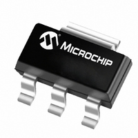
TC1262-3.3VDBTR Microchip Technology, TC1262-3.3VDBTR Datasheet - Page 3

TC1262-3.3VDBTR
Manufacturer Part Number
TC1262-3.3VDBTR
Description
IC CMOS LDO 3.3V 500MA SOT223-3
Manufacturer
Microchip Technology
Datasheet
1.TC1262-3.3VDBTR.pdf
(12 pages)
Specifications of TC1262-3.3VDBTR
Package / Case
SOT-223 (3 leads + Tab), SC-73, TO-261
Regulator Topology
Positive Fixed
Voltage - Output
3.3V
Voltage - Input
Up to 6V
Voltage - Dropout (typical)
0.35V @ 500mA
Number Of Regulators
1
Current - Output
500mA (Min)
Operating Temperature
-40°C ~ 125°C
Mounting Type
Surface Mount
Number Of Outputs
1
Polarity
Positive
Input Voltage Max
6 V
Output Voltage
3.3 V
Output Type
Fixed
Dropout Voltage (max)
650 mV
Output Current
500 mA
Line Regulation
0.003 % / V
Load Regulation
0.002 % / mA
Voltage Regulation Accuracy
0.5 %
Maximum Operating Temperature
+ 125 C
Mounting Style
SMD/SMT
Minimum Operating Temperature
- 40 C
Primary Input Voltage
6V
Output Voltage Fixed
3.3V
Dropout Voltage Vdo
350mV
No. Of Pins
3
Operating Temperature Range
-40°C To +125°C
Rohs Compliant
Yes
Lead Free Status / RoHS Status
Lead free / RoHS Compliant
Current - Limit (min)
-
Lead Free Status / Rohs Status
Lead free / RoHS Compliant
Other names
TC12623.3VDBTR
Available stocks
Company
Part Number
Manufacturer
Quantity
Price
Company:
Part Number:
TC1262-3.3VDBTR
Manufacturer:
Microchip Technology
Quantity:
36 582
Company:
Part Number:
TC1262-3.3VDBTR
Manufacturer:
TELCOM
Quantity:
4 656
Part Number:
TC1262-3.3VDBTR
Manufacturer:
MICROCHIP/微芯
Quantity:
20 000
2.0
The descriptions of the pins are listed in Table 2-1.
TABLE 2-1:
3.0
The TC1262 is a precision, fixed output LDO. Unlike
bipolar regulators, the TC1262’s supply current does
not increase with load current. In addition, V
remains stable and within regulation over the entire
0mA to I
consideration in RTC and CMOS RAM battery back-up
applications).
Figure 3-1 shows a typical application circuit.
FIGURE 3-1:
©
(3-Pin SOT-223)
(3-Pin DDPAK)
(3-Pin TO-220)
Battery
2002 Microchip Technology Inc.
Pin No.
1
2
3
PIN DESCRIPTIONS
DETAILED DESCRIPTION
LOAD
+
–
MAX
+
PIN FUNCTION TABLE
C1
1µF
load current range (an important
Symbol
V
GND
V
OUT
TYPICAL APPLICATION
CIRCUIT
IN
V
GND
IN
TC1262
Unregulated supply input.
Ground terminal.
Regulated voltage output.
V
OUT
+
C2
1µF
V
OUT
OUT
3.1
A 1µF (min) capacitor from V
The output capacitor should have an effective series
resistance greater than 0.1Ω and less than 5Ω, and a
resonant frequency above 1MHz. A 1µF capacitor
should be connected from V
than 10 inches of wire between the regulator and the
AC filter capacitor, or if a battery is used as the power
source. Aluminum electrolytic or tantalum capacitor
types can be used. (Since many aluminum electrolytic
capacitors freeze at approximately -30°C, solid
tantalums are recommended for applications operating
below -25°C.) When operating from sources other than
batteries,
response can be improved by increasing the value of
the input and output capacitors and employing passive
filtering techniques.
Description
Output Capacitor
supply-noise
rejection
IN
OUT
to GND if there is more
to ground is required.
TC1262
DS21373B-page 3
and
transient


