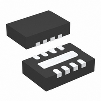
LT1965EDD-3.3#PBF Linear Technology, LT1965EDD-3.3#PBF Datasheet

LT1965EDD-3.3#PBF
Specifications of LT1965EDD-3.3#PBF
Available stocks
Related parts for LT1965EDD-3.3#PBF
LT1965EDD-3.3#PBF Summary of contents
Page 1
... The package offerings include the 5-lead TO-220, 5-lead DD-PAK as well as the thermally enhanced 8-lead MSOP and low-profi le (0.75mm) 8-lead 3mm × 3mm DFN. L, LT, LTC and LTM are registered trademarks of Linear Technology Corporation. All other trademarks are the property of their respective owners. 400 350 2 ...
Page 2
... LT1965IDD-1.5#TRPBF LT1965EDD-1.8#PBF LT1965EDD-1.8#TRPBF LT1965IDD-1.8#PBF LT1965IDD-1.8#TRPBF LT1965EDD-2.5#PBF LT1965EDD-2.5#TRPBF LT1965IDD-2.5#PBF LT1965IDD-2.5#TRPBF LT1965EDD-3.3#PBF LT1965EDD-3.3#TRPBF LT1965IDD-3.3#PBF LT1965IDD-3.3#TRPBF 2 Output Short-Circuit Duration .......................... Indefi nite Operating Junction Temperature Range (E, I Grade) (Notes 2, 13) ......................................–40°C to 125°C Storage Temperature Range ...................–65°C to 150°C Lead Temperature (Soldering, 10 sec) (Only for MSOP , TO-220, DD-PAK Packages) .... 300° ...
Page 3
ORDER INFORMATION LEAD FREE FINISH TAPE AND REEL LT1965EMS8E#PBF LT1965EMS8E#TRPBF LT1965IMS8E#PBF LT1965IMS8E#TRPBF LT1965EMS8E-1.5#PBF LT1965EMS8E-1.5#TRPBF LTDKX LT1965IMS8E-1.5#PBF LT1965IMS8E-1.5#TRPBF LTDKX LT1965EMS8E-1.8#PBF LT1965EMS8E-1.8#TRPBF LTDKZ LT1965IMS8E-1.8#PBF LT1965IMS8E-1.8#TRPBF LTDKZ LT1965EMS8E-2.5#PBF LT1965EMS8E-2.5#TRPBF LTDMC LT1965IMS8E-2.5#PBF LT1965IMS8E-2.5#TRPBF LTDMC LT1965EMS8E-3.3#PBF LT1965EMS8E-3.3#TRPBF LTDMF LT1965IMS8E-3.3#PBF LT1965IMS8E-3.3#TRPBF LTDMF LT1965EQ#PBF LT1965EQ#TRPBF LT1965IQ#PBF LT1965IQ#TRPBF ...
Page 4
LT1965 Series ELECTRICAL CHARACTERISTICS temperature range, otherwise specifi cations are at T PARAMETER Minimum Input Voltage (Notes 4, 12) Regulated Output Voltage (Note 5) ADJ Pin Voltage (Notes 4, 5) Line Regulation Load Regulation Dropout Voltage ...
Page 5
ELECTRICAL CHARACTERISTICS temperature range, otherwise specifi cations are at T PARAMETER Current Limit Input Reverse Leakage Current Reverse Output Current (Note 11) Note 1: Stresses beyond those listed under Absolute Maximum Ratings may cause permanent damage to the device. Exposure ...
Page 6
LT1965 Series TYPICAL PERFORMANCE CHARACTERISTICS Typical Dropout Voltage 500 450 400 T = 125°C 350 J 300 250 200 T = 25°C J 150 100 0.2 0.6 0.8 1 0.4 OUTPUT CURRENT (A) 1965 G01 Quiescent Current ...
Page 7
TYPICAL PERFORMANCE CHARACTERISTICS LT1965-1.5 Quiescent Current 25° ∞ SHDN SHDN INPUT ...
Page 8
LT1965 Series TYPICAL PERFORMANCE CHARACTERISTICS LT1965-2.5 GND Pin Current (Light Load 25° SHDN 10 *FOR V = 2.5V OUT 250Ω 10mA 2.5k, ...
Page 9
TYPICAL PERFORMANCE CHARACTERISTICS SHDN Pin Input Current SHDN PIN VOLTAGE (V) 1965 G11 Current Limit vs V – OUT 2.5 ΔV ...
Page 10
LT1965 Series TYPICAL PERFORMANCE CHARACTERISTICS Ripple Rejection vs Temperature 100 0.75A 0.5 IN OUT(NOMINAL) P-P RIPPLE 120Hz 60 –50 – 100 ...
Page 11
PIN FUNCTIONS (DFN/MSOP/DD-PAK/TO-220) OUT (Pins 4): Output. This pin supplies power to the load. Use a minimum output capacitor of 10μF to prevent oscillations. Large load transient applica- tions require larger output ...
Page 12
... The ADJ pin bias current, 1.3μA at 25°C, fl ows through R2 into the ADJ pin. Use the formula in Figure 2 to calcu- late output voltage. Linear Technology recommends that R1’s value be less than 12.1k to minimize output voltage errors due to the ADJ pin bias current. In shutdown, the output turns off and the divider current is zero ...
Page 13
APPLICATIONS INFORMATION capacitor values below appropriate levels. Capacitor DC bias characteristics tend to improve as component case size increases, but expected capacitance at operating voltages should be verifi ed. Voltage and temperature coeffi cients are not the only sources of ...
Page 14
LT1965 Series APPLICATIONS INFORMATION recover. Other regulators, such as the LT1083/LT1084/ LT1085 family, also exhibit this phenomenon not unique to the LT1965. The problem occurs with a heavy output load when the input voltage is high and ...
Page 15
APPLICATIONS INFORMATION The following tables list thermal resistance for several different board sizes and copper areas. All measurements were taken in still air on 1/16" FR-4 board with one ounce copper. Table 1. Measured Thermal Resistance for DFN Package Copper ...
Page 16
LT1965 Series APPLICATIONS INFORMATION Protection Features The LT1965 regulators incorporate several protection features that makes them ideal for use in battery-powered circuits. In addition to the normal protection features associated with monolithic regulators, such as current limiting and thermal limiting, ...
Page 17
TYPICAL APPLICATIONS + V > 3.7V IN Paralleling of Regulators for Higher Output Current R1 0.01Ω IN OUT C1 LT1965-3.3 100μF SHDN SENSE GND R2 0.01Ω IN OUT LT1965 SHDN SHDN ADJ GND R3 R4 2.2k 2. ...
Page 18
LT1965 Series PACKAGE DESCRIPTION 3.5 ±0.05 1.65 ±0.05 2.15 ±0.05 (2 SIDES) 0.25 ± 0.05 0.50 BSC 2.38 ±0.05 (2 SIDES) RECOMMENDED SOLDER PAD PITCH AND DIMENSIONS NOTE: 1. DRAWING TO BE MADE A JEDEC PACKAGE OUTLINE M0-229 VARIATION OF ...
Page 19
... BSC (1.70) Information furnished by Linear Technology Corporation is believed to be accurate and reliable. However, no responsibility is assumed for its use. Linear Technology Corporation makes no representa- tion that the interconnection of its circuits as described herein will not infringe on existing patent rights. Q Package 5-Lead Plastic DD Pak (Reference LTC DWG # 05-08-1461) .390 – ...
Page 20
... LT3028 Dual, 100mA/500mA, Low Noise Micropower, LDO with Independent Inputs LT3080/ 1.1A Parallelable, Low Noise, Low Dropout LT3080-1 Linear Regulator ThinSOT is a trademark of Linear Technology Corporation 20 Linear Technology Corporation 1630 McCarthy Blvd., Milpitas, CA 95035-7417 (408) 432-1900 FAX: (408) 434-0507 ● Adjustable Current Source R5, 0.01Ω ...


