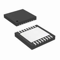
LT3021EDH#PBF Linear Technology, LT3021EDH#PBF Datasheet - Page 5

LT3021EDH#PBF
Manufacturer Part Number
LT3021EDH#PBF
Description
IC REG LDO ADJ 500MA 16-DFN
Manufacturer
Linear Technology
Datasheet
1.LT3021ES8PBF.pdf
(16 pages)
Specifications of LT3021EDH#PBF
Regulator Topology
Positive Adjustable
Voltage - Output
0.2 ~ 9.5 V
Voltage - Input
0.9 ~ 10 V
Voltage - Dropout (typical)
0.155V @ 500mA
Number Of Regulators
1
Current - Output
500mA
Current - Limit (min)
550mA
Operating Temperature
-40°C ~ 125°C
Mounting Type
Surface Mount
Package / Case
16-DFN
Lead Free Status / RoHS Status
Lead free / RoHS Compliant
Available stocks
Company
Part Number
Manufacturer
Quantity
Price
ELECTRICAL CHARACTERISTICS
temperature range, otherwise specifi cations are at T
Note 1: Stresses beyond those listed under Absolute Maximum Ratings
may cause permanent damage to the device. Exposure to any Absolute
Maximum Rating condition for extended periods may affect device
reliability and lifetime.
Note 2: The LT3021 regulators are tested and specifi ed under pulse load
conditions such that T
at T
characterization and correlation with statistical process controls. The
LT3021I regulators are guaranteed over the full –40ºC to 125ºC operating
junction temperature range.
Note 3: This IC includes overtemperature protection that is intended
to protect the device during momentary overload conditions. Junction
temperature will exceed 125°C when overtemperature protection is active.
Continuous operation above the specifi ed maximum operating junction
temperature may impair device reliability.
Note 4: Maximum junction temperature limits operating conditions. The
regulated output voltage specifi cation does not apply for all possible
combinations of input voltage and output current. Limit the output current
range if operating at maximum input voltage. Limit the input voltage range
if operating at maximum output current.
Note 5: Typically the LT3021 supplies 500mA output current with a 1V
input supply. The guranteed minimum input voltage for 500mA output
current is 1.10V.
Note 6: The LT3021 is tested and specifi ed for these conditions with an
external resistor divider (20k and 30.1k) setting V
resistor divider adds 10μA of output load current. The line regulation and
load regulation specifi cations refer to the change in the 0.2V reference
TYPICAL PERFORMANCE CHARACTERISTICS
A
250
225
200
175
150
125
100
75
50
25
= 25°C. Performance at –40°C and 125°C is assured by design,
0
0
Dropout Voltage
100
OUTPUT CURRENT (mA)
J
200
≈ T
A
T
. The LT3021E regulators are 100% tested
J
= 125°C
300
T
J
= 25°C
400
3021 G01
500
OUT
to 0.5V. The external
250
225
200
175
150
125
100
75
50
25
0
–50
J
Dropout Voltage
V
= 25°C.
OUT
–25
= 1.2V
The
0
TEMPERATURE (°C)
l
denotes the specifi cations which apply over the full operating
25
voltage, not the 0.5V output voltage. Specifi cations for fi xed output voltage
devices are referred to the output voltage.
Note 7: Dropout voltage is the minimum input to output voltage differential
needed to maintain regulation at a specifi ed output current. In dropout the
output voltage equals: (V
Note 8: GND pin current is tested with V
current source load. GND pin current will increase in dropout. See GND pin
current curves in the Typical Performance Characteristics section.
Note 9: Adjust pin bias current fl ows out of the ADJ pin.
Note 10: Shutdown pin current fl ows into the SHDN pin.
Note 11: Reverse output current is tested with IN grounded and OUT
forced to the rated output voltage. This current fl ows into the OUT pin and
out of the GND pin. For fi xed voltage devices this includes the current in
the output resistor divider.
Note 12: The LT3021 is tested and specifi ed for these conditions with an
external resistor divider (20k and 100k) setting V
resistor divider adds 10μA of load current.
Note 13: Reverse current is higher for the case of (rated_output) < V
< V
trying to restore the output voltage to its nominal value.
Note 14: Minimum input voltage is the minimum voltage required by the
control circuit to regulate the output voltage and supply the full 500mA
rated current. This specifi cation is tested at V
voltages the minimum input voltage required for regulation will be equal to
the regulated output voltage V
50
IN,
because the no-load recovery circuitry is active in this region and is
75
I
I
I
L
L
L
I
= 500mA
= 250mA
= 100mA
L
I
L
I
L
= 50mA
= 10mA
= 1mA
100
3021 G02
LT3021-1.5/LT3021-1.8
125
LT3021/LT3021-1.2/
IN
– V
1.2
1.1
1.0
0.9
0.8
0.7
0.6
0.5
0.4
0.3
0.2
OUT
DROPOUT
–50
Minimum Input Voltage
I
plus the dropout voltage.
L
= 500mA
–25
).
IN
= V
0
TEMPERATURE (°C)
OUT
OUT(NOMINAL)
OUT
25
= 0.5V. At higher output
to 1.2V. The external
50
+ 0.4V and a
75
100
3021 G16
OUT
3021fc
5
125


