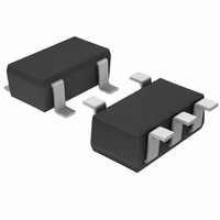
BH18LB1WG-TR Rohm Semiconductor, BH18LB1WG-TR Datasheet - Page 5

BH18LB1WG-TR
Manufacturer Part Number
BH18LB1WG-TR
Description
IC REG LDO 150MA 1.8V SHDN 5SSOP
Manufacturer
Rohm Semiconductor
Series
-r
Specifications of BH18LB1WG-TR
Regulator Topology
Positive Fixed
Voltage - Output
1.8V
Voltage - Input
2.5 ~ 5.5 V
Number Of Regulators
1
Current - Output
150mA (Max)
Operating Temperature
-40°C ~ 85°C
Mounting Type
Surface Mount
Package / Case
5-SSOP
Primary Input Voltage
5.5V
Output Voltage
1.8V
No. Of Pins
5
Output Current
150mA
Voltage Regulator Case Style
SSOP
Operating Temperature Range
-40°C To +85°C
Svhc
No SVHC (18-Jun-2010)
Base
RoHS Compliant
Number Of Outputs
1
Polarity
Positive
Input Voltage Max
5.5 V
Output Type
Fixed
Line Regulation
20 mV
Load Regulation
90 mV
Voltage Regulation Accuracy
1 %
Maximum Power Dissipation
0.54 W
Maximum Operating Temperature
+ 85 C
Mounting Style
SMD/SMT
Minimum Operating Temperature
- 40 C
Output Voltage Fixed
1.8V
Rohs Compliant
Yes
Featured Product
CMOS LDO Regulators
Voltage - Dropout (typical)
-
Current - Limit (min)
-
Lead Free Status / RoHS Status
Lead free / RoHS Compliant
Voltage - Dropout (typical)
-
Current - Limit (min)
-
Lead Free Status / Rohs Status
Lead free / RoHS Compliant
Available stocks
Company
Part Number
Manufacturer
Quantity
Price
Company:
Part Number:
BH18LB1WG-TR
Manufacturer:
HITACHI
Quantity:
27
Part Number:
BH18LB1WG-TR
Manufacturer:
ROHM/罗姆
Quantity:
20 000
2.
www.rohm.com
© 2010 ROHM Co., Ltd. All rights reserved.
BH □□FB1WG series, BH□□FB1WHFV series,
BH □□LB1WG series, BH□□LB1WHFV series, BH □□MA3WHFV series
Power dissipation
Block diagrams
Power dissipation Pd
1. Power dissipation
Power Dissipation Reduction (Example)
Power dissipation calculation include estimates of power dissipation characteristics and internal IC power consumption
and should be treated as guidelines. In the event that the IC is used in an environment where this power dissipation is
exceeded, the attendant rise in the junction temperature will trigger the thermal shutdown circuit, reducing the current
capacity and otherwise degrading the IC's design performance. Allow for sufficient margins so that this power dissipation
is not exceeded during IC operation.
Calculating the maximum internal IC power consumption (P
Fig. 26: HVSOF6
Power Dissipation/
Board: 70 mm
Material: Glass epoxy PCB
characteristics (Pd)
°
X
70 mm
X
1.6 mm
Power Dissipation Reduction (Example)
Fig. 27: HVSOF5
Power Dissipation/
Board: 70 mm
Material: Glass epoxy PCB
5/8
°
X
70 mm
MAX
)
X
1.6 mm
Terminal No. Terminal Name Function
Input voltage
Output voltage
Output current
Power Dissipation Reduction (Example)
Output voltage ON/OFF control
(High: ON, Low: OFF)
Ground
Power supply input
Voltage output
NO CONNECT
Power Dissipation/
Power supply input
Ground
Output voltage ON/OFF control
(High: ON, Low: OFF)
NO CONNECT
Voltage output
Power supply input
Voltage output
Voltage output
Noise reducing capacitor
ground terminal
Ground
Output voltage ON/OFF control
(High: ON, Low: OFF)
Board: 70 mm
Material: Glass epoxy PCB
Fig. 28: SSOP5
Technical Note
2010.07 - Rev. C
°
X
70 mm
X
1.6 mm


