XC6210B332MR Torex Semiconductor Ltd, XC6210B332MR Datasheet
XC6210B332MR
Specifications of XC6210B332MR
Available stocks


Related parts for XC6210B332MR


XC6210B332MR Summary of contents
Page 1
XC6210 Series High Current, High Speed LDO Regulators ■GENERAL DESCRIPTION The XC6210 series are precise, low noise, high current, positive voltage low dropout regulators. They are fabricated using Torex’s CMOS process. The series features a voltage reference, an error amplifier, ...
Page 2
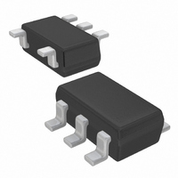
XC6210 Series ■PIN CONFIGURATION V NC OUT SOT-89-5 SOT-25 (TOP VIEW) (TOP VIEW) ■PIN ASSIGNMENT PIN NUMBER SOT-25 SOT-89 ■LOGIC ...
Page 3
FUNCTION ASSIGNMENT 1) XC6210A Type (CE High Active、CE CE "H" Level "L" Level "OPEN" 2) XC6210B Type (CE High Active、CE CE "H" Level "L" Level "OPEN" 3) XC6210C Type (CE Low Active、CE CE "H" Level "L" Level "OPEN" 4) ...
Page 4
XC6210 Series ■BLOCK DIAGRAM XC6210Aシリーズ XC6210A Series XC6210Cシリーズ XC6210C Series ※ 上図のダイオードは静電保護用と寄生のダイオードになります。 Diodes shown in the above circuit are ESD protection diodes and parasitic diodes * ■ABSOLUTE MAXIMUM RATINGS PARAMETER Input Voltage Output Current * Output Voltage CE Pin Voltage ...
Page 5
CHARACTERISTICS ●XC6210 series PARAMETER SYMBOL (*3) Output Voltage V OUT(E) Maximum Output Current I OUTMAX Load Regulation △V OUT (*4) Vdif1 Dropout Voltage (*4) Vdif2 Supply Current (A type) Supply Current (B type Supply Current (C type) ...
Page 6
XC6210 Series ■VOLTAGE CHART ●Dropout Voltage, Supply Current, CE “H / L” Level Current Chart SETTING OUTPUT DROPOUT OUTPUT VOLTAGE VOLTAGE 1 VOLTAGE (I (V) (V) V OUT V OUT(T) MIN. MAX. TYP. 0.80 0.770 0.830 0.85 0.820 0.880 100.0 ...
Page 7
CHART (Continued) ●Dropout Voltage, Supply Current, CE “H / L” Level Current Chart SETTING OUTPUT DROPOUT OUTPUT VOLTAGE VOLTAGE 1 VOLTAGE (I OUT (V) (V) V OUT V OUT(T) MIN. MAX. TYP. 3.00 2.940 3.060 3.05 2.989 3.111 3.10 ...
Page 8
XC6210 Series ■TEST CIRCUITS ●Circuit① (Output Voltage, Maximum Output Voltage, Load Regulation, Dropout Voltage, Line Regulation, Output Voltage Temperature Characteristics, Current Limiter, Short-Circuit Current, CE “H” “L” Level Voltage, CE “H” “L” Level Current) V ●Circuit ② (Supply Current, Stand-by ...
Page 9
EXPLANATION <Output Voltage Regulator Control> The voltage, divided by resistors R1 & R2, which are connected to the V voltage by the error amplifier. The P-channel MOSFET, which is connected to the V subsequent output signal. The output voltage ...
Page 10
XC6210 Series ■NOTES ON USE 1. Please use this IC within the stated absolute maximum ratings. For temporary, transitional voltage drop or voltage rising phenomenon, the IC is liable to malfunction should the ratings be exceeded. 2. Where wiring impedance ...
Page 11
PERFORMANCE CHARACTERISTICS (1) Output Voltage vs. Output Current XC6210x082xx C =1.0μF(ceramic),C IN 0.9 0.8 0.7 Ta=-40 ℃ 0.6 Ta=25 ℃ 0.5 Ta=85 ℃ 0.4 0.3 0.2 0 100 200 300 400 500 600 700 800 900 Output ...
Page 12
XC6210 Series ■TYPICAL PERFORMANCE CHARACTERISTICS (Continued) (2) Output Voltage vs. Input Voltage XC6210x082xx C =1.0μF(ceramic),C IN 1.1 1.0 0.9 0.8 0.7 0.6 0.5 0.5 1.0 1.5 Input Voltage : V XC6210x302xx C =1.0μF(ceramic),C IN 3.2 3.0 2.8 2.6 2.4 2.2 ...
Page 13
PERFORMANCE CHARACTERISTICS (Continued) (3) Dropout Voltage vs. Output Current XC6210x082xx C =1.0μF(ceramic),C IN 1.0 0.9 0.8 0.7 Below the minimum operating voltage 0.6 0.5 0.4 0.3 0.2 0.1 0.0 0 100 200 300 Output Current : I OUT XC6210x152xx ...
Page 14
XC6210 Series ■TYPICAL PERFORMANCE CHARACTERISTICS (Continued) (4) Supply Current vs. Input Voltage XC6210x082xx C =1.0μF(ceramic),C IN 100 0.0 1.0 2.0 3.0 Input Voltage : V IN XC6210x502xx C =1.0μF(ceramic),C 120 IN 100 80 60 Ta=85 ...
Page 15
PERFORMANCE CHARACTERISTICS (Continued) (6) Supply Current vs. Ambient Temperature XC6210x082xx C =1.0μF(ceramic), -50 - Ambient Temperature : Topr( ℃ ) XC6210x502xx C =1.0μF(ceramic), ...
Page 16
XC6210 Series ■TYPICAL PERFORMANCE CHARACTERISTICS (Continued) (8) Input Transient Response 1 XC6210x082xx I OUT C =6.8μF(ceramic),Ta=25 ℃ L 1.2 Input Voltage 1.1 1.0 0.9 0.8 0.7 Output Voltage 0.6 Time (20μs/div ) XC6210x302xx I OUT C =1.0μF(ceramic),Ta=25 ℃ L 3.4 ...
Page 17
PERFORMANCE CHARACTERISTICS (Continued) (9) Load Transient Response XC6210x082xx V =1.8V,tr=tf=5.0μs,Ta=25 ℃ =1.0μF(ceramic),C =6.8μF(ceramic 1.0 Output Voltage 0.8 0.6 0.4 Output Current 100mA 0.2 10mA 0.0 Time (25μs/div ) XC6210x302xx V =4.0V,tr=tf=5.0μs,Ta=25 ℃ =1.0μF(ceramic),C ...
Page 18
XC6210 Series ■TYPICAL PERFORMANCE CHARACTERISTICS (Continued) (10) Ripple Rejection Rate XC6210x082xx V =1.8V +0. P-PAC C =1.0μF(ceramic), 0.01 0.1 1 Ripple Frequency : f (kHz) XC6210x502xx V =5.75V ...
Page 19
PERFORMANCE CHARACTERISTICS (Continued) (11) Input Transient Response 2 XC6210x082xx V =1.8V,I IN OUT C =1.0μF(ceramic),C =6.8μF(ceramic),Ta=25 ℃ 5.0 CE Input Voltage 4.0 3.0 2.0 Output Voltage 1.0 0.0 Time (25μs/div ) XC6210x302xx V =4.0V,I IN OUT C ...
Page 20
XC6210 Series ■PACKAGING INFORMATION ●SOT-25 ●USP-6B 20/27 ●SOT-89-5 (unit : mm) (unit : mm) (unit : mm) ...
Page 21
INFORMATION (Continued) ●USP-6B Reference Pattern Layout ●USP-6B Reference Metal Mask Design (unit : mm) XC6210 Series (unit : mm) 21/27 ...
Page 22
XC6210 Series ■PACKAGING INFORMATION (Continued) ●SOT-25 Power Dissipation Power dissipation data for the SOT-25 is shown in this page. The value of power dissipation varies with the mount board conditions. Please use this data as one of reference data taken ...
Page 23
INFORMATION (Continued) ● SOT-89-5 Power Dissipation Power dissipation data for the SOT-89-5 is shown in this page. The value of power dissipation varies with the mount board conditions. Please use this data as one of reference data taken in ...
Page 24
XC6210 Series ■PACKAGING INFORMATION (Continued) ● USP-6B Power Dissipation Power dissipation data for the USP-6B is shown in this page. The value of power dissipation varies with the mount board conditions. Please use this data as one of reference data ...
Page 25
RULE ●SOT-25 ●SOT-89-5 SOT-89-5 (TOP VIEW) ① represents product series MARK 0 ② represents CE function MARK OUTPUT OUTPUT OUTPUT VOLTAGE= VOLTAGE= VOLTAGE= 0.80~3.00V 3.10~5.00V 0.85~3.05V ③ ...
Page 26
XC6210 Series ■MARKING RULE (Continued) ●USP-6B ①② represents product series ③ represents CE Function USP-6B (TOP VIEW) ④ represents the integer number of output voltage ⑤ represents the decimal point of output voltage MARK ⑥ represents production lot number 0 ...
Page 27
... Should you wish to use the products under conditions exceeding the specifications, please consult us or our representatives assume no responsibility for damage or loss due to abnormal use. 7. All rights reserved. No part of this datasheet may be copied or reproduced without the prior permission of TOREX SEMICONDUCTOR LTD. XC6210 Series 27/27 ...