BD10KA5WFP-E2 Rohm Semiconductor, BD10KA5WFP-E2 Datasheet - Page 2
BD10KA5WFP-E2
Manufacturer Part Number
BD10KA5WFP-E2
Description
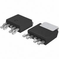
IC REG LDO 500MA 1.0V TO252-5
Manufacturer
Rohm Semiconductor
Datasheet
1.BD10KA5WFP-E2.pdf
(10 pages)
Specifications of BD10KA5WFP-E2
Regulator Topology
Positive Fixed
Voltage - Output
1V
Voltage - Input
2.3 ~ 5.5 V
Number Of Regulators
1
Current - Output
500mA (Max)
Operating Temperature
-40°C ~ 105°C
Mounting Type
Surface Mount
Package / Case
TO-252-4, DPak (4 Leads + Tab), TO-252AD
Number Of Outputs
1
Polarity
Positive
Input Voltage Max
5.5 V
Output Voltage
1 V
Output Type
Fixed
Output Current
500 mA
Line Regulation
35 mV
Load Regulation
75 mV
Voltage Regulation Accuracy
1 %
Maximum Power Dissipation
1.3 W
Maximum Operating Temperature
+ 105 C
Mounting Style
SMD/SMT
Minimum Operating Temperature
- 40 C
Lead Free Status / RoHS Status
Lead free / RoHS Compliant
Voltage - Dropout (typical)
-
Current - Limit (min)
-
Lead Free Status / Rohs Status
Lead free / RoHS Compliant
Other names
BD10KA5WFP-E2TR
Available stocks
Company
Part Number
Manufacturer
Quantity
Price

Part Number:
BD10KA5WFP-E2
Manufacturer:
ROHM/罗姆
Quantity:
20 000


●Absolute Maximum Ratings(Ta=25℃)
●Recommended Operating Range (Ta=25℃)
●Electrical Characteristics (abridged)
© 2009 ROHM Co., Ltd. All rights reserved.
BD□□KA5,BD□□KA5W Series,BD00KA5W Series
www.rohm.com
BD□□KA5WFP / WF / FP
(Unless specified otherwise,Ta=25℃,V
BD00KA5WFP / WF
(Unless specified otherwise, Ta=25℃, Vcc=2.5V,VL=2V,R1=30kΩ,R2=30kΩ
Power Supply Voltage
Output Control Terminal Voltage
Power Dissipation
Operating Temperature Range
Ambient Storage Temperature
Maximum Junction Temperature
Input Power Supply Voltage
Output Current
Output Voltage Configuration Range
Output Control Terminal Voltage
Output Voltage
Circuit Current at Shutdown
Minimum I/O Voltage
Difference
Output Current Capacity
Input Stability
Load Stability
Output Voltage
Temperature Coefficient
Circuit Current at Shutdown
Reference Voltage
Minimum I/O Voltage
Difference*10
Output Current Capacity
Input Stability
Load Stability
Output Voltage
Temperature Coefficient
*1 Must not exceed Pd
*2 When a 70mm×70mm×1.6mm glass epoxy board is used. Reduce by 9.6 mW/℃ over 25℃.
*3 When a 70mm×70mm×1.6mm glass epoxy board is used. Reduce by 10.4mW/℃ over 25℃.
*4 When a 70mm×70mm×1.6mm glass epoxy board is used. Reduce by 5.5 mW/℃ over 25℃.
*5 Only BD00KA5WFP and BD00KA5WF
Vo(T):Preset output voltage value
*6 When Vo≧2.5V
*7 When 1.0≦Vo≦1.8V, Vcc=2.3V→5.5V
*8 Design guarantee(100% shipping inspection not performed)
*9
*10
*11
VOUT=VADJ×(R1+R2)÷R1(V)
VADJ×0.75V(Typ.)
When Vo≧2.5V
Design guarantee(100% shipping inspection not performed)
Parameter
Parameter
*6
Parameter
Parameter
*7
TO252-3
TO252-5
SOP8
*8
*11
Symbol
Symbol
Reg.L
Reg.L
Reg.I
Reg.I
ΔVd
ΔVd
Tcvo
Tcvo
V
*5
Isd
Isd
Vo
Io
Io
ADJ
CTL
=2V,Vcc=2.5V(Vo=1.0V,1.2V,1.5V,1.8V),Vcc=3.3V(Vo=2.5V),Vcc=5.0V(Vo=3.0V,3.3V))
Vo(T)×0.99
Vo(T)-0.015
Symbol
Symbol
Tjmax
V
V
Topr
Tstg
Vcc
Vcc
Pd
Vo
0.742
CTL
Io
CTL
Min.
Min.
500
500
-
-
-
-
-
-
-
-
-
-
±100
±100
Vo(T)
Vo(T)
0.750
2/9
Typ.
0.12
Typ.
0.12
10
25
10
25
0
0
-
-
Min.
2.3
1.0
0
0
-0.3~+7.0
-0.3~Vcc
-40~+105
-55~+150
Vo(T)+0.015
687.6
Vo(T)×1.01
1200
1300
Limits
150
0.758
Max.
Max.
0.20
0.20
35
75
35
75
*2
*3
*4
1
1
-
-
-
-
*1
*1
Max.
500
Vcc
5.5
4.0
*9
)
ppm/℃
ppm/℃
Unit.
Unit.
mA
mV
mV
mA
mV
mV
μA
μA
V
V
V
V
V
Unit.
Unit.
mW
mA
℃
℃
℃
V
V
V
V
V
Io=200mA (Vo=1.0V,1.2V)
Io=200mA (Vo≧1.5V)
V
(during OFF mode)
Io=200mA,Vcc=0.95×Vo
Vcc=Vo+0.5V→5.5V,Io=200mA
Io=0mA→500mA
Io=5mA,Tj=0~125℃
V
(during OFF mode)
Io=50mA
Io=200mA,Vcc=0.95×Vo
Vcc=Vo+0.5V→5.5V,Io=200mA
Io=0mA→500mA
Io=5mA,Tj=0~125℃
CTL
CTL
=0V,Io=0mA
=0V, Io=0mA
Technical Note
2009.04 - Rev.A
Conditions
Conditions
Related parts for BD10KA5WFP-E2
Image
Part Number
Description
Manufacturer
Datasheet
Request
R

Part Number:
Description:
Manufacturer:
Rohm Semiconductor
Datasheet:
Part Number:
Description:
Manufacturer:
Rohm Semiconductor
Datasheet:
Part Number:
Description:
Manufacturer:
Rohm Semiconductor
Datasheet:
Part Number:
Description:
Manufacturer:
Rohm Semiconductor
Datasheet:
Part Number:
Description:
Manufacturer:
Rohm Semiconductor
Datasheet:
Part Number:
Description:
Manufacturer:
Rohm Semiconductor
Datasheet:
Part Number:
Description:
Manufacturer:
Rohm Semiconductor
Datasheet:
Part Number:
Description:
Manufacturer:
Rohm Semiconductor
Datasheet:
Part Number:
Description:
Manufacturer:
Rohm Semiconductor
Datasheet:
Part Number:
Description:
Manufacturer:
Rohm Semiconductor
Datasheet:
Part Number:
Description:
Manufacturer:
Rohm Semiconductor
Datasheet:
Part Number:
Description:
Manufacturer:
Rohm Semiconductor
Datasheet:

Part Number:
Description:
DIODE SWITCH 80V 25MA SMD5 TR
Manufacturer:
Rohm Semiconductor
Datasheet: