ADP125ARHZ-R7 Analog Devices Inc, ADP125ARHZ-R7 Datasheet
ADP125ARHZ-R7
Specifications of ADP125ARHZ-R7


Related parts for ADP125ARHZ-R7


ADP125ARHZ-R7 Summary of contents
Page 1
FEATURES Input voltage supply range: 2 5.5 V 500 mA maximum output current Fixed and adjustable output voltage versions 1% initial accuracy fixed-output voltage options available from 1. 3.3 V Adjustable-output voltage range ...
Page 2
ADP124/ADP125 TABLE OF CONTENTS Features .............................................................................................. 1 Applications ....................................................................................... 1 Typical Application Circuits ............................................................ 1 General Description ......................................................................... 1 Revision History ............................................................................... 2 Specifications ..................................................................................... 3 Recommended Capacitor Specifications ................................... 4 Absolute Maximum Ratings ............................................................ 5 Thermal Data ................................................................................ 5 ...
Page 3
SPECIFICATIONS Unless otherwise noted 0 2.3 V, whichever is greater; ADJ connected to VOUT OUT = 1.0 µ 25°C. OUT A Table 1. Parameter Symbol INPUT VOLTAGE RANGE V ...
Page 4
ADP124/ADP125 Parameter Symbol OUTPUT NOISE OUT POWER SUPPLY REJECTION RATIO PSRR ( +1V) IN OUT 1 The current from the external resistor divider network in the case of adjustable voltage output (as with the ADP125) should be subtracted ...
Page 5
ABSOLUTE MAXIMUM RATINGS Table 3. Parameter VIN to GND ADJ to GND EN to GND VOUT to GND Storage Temperature Range Operating Ambient Temperature Range Operating Junction Temperature Range Soldering Conditions Stresses above those listed under Absolute Maximum Ratings may ...
Page 6
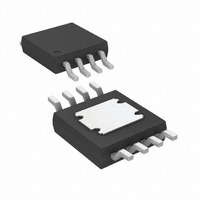
ADP124/ADP125 PIN CONFIGURATIONS AND FUNCTION DESCRIPTIONS VOUT 1 8 ADP124 VOUT 2 7 TOP VIEW VOUT SENSE 3 6 (Not to Scale) GND 4 5 NOTES CONNECT. 2. THE EXPOSED PAD MUST BE CONNECTED TO GROUND. ...
Page 7
TYPICAL PERFORMANCE CHARACTERISTICS 3.3V mA OUT OUT 3.310 3.305 3.300 3.295 I = 100µA 3.290 OUT I = 1mA OUT I = 10mA OUT 3.285 I = 100mA OUT ...
Page 8
ADP124/ADP125 0.7 0 5. 4.20 0 3.80 IN 0.2 0.1 0 –50 –25 0 ...
Page 9
I = 100µA OUT – 1mA OUT I = 10mA OUT I = 100mA –40 OUT I = 300mA OUT I = 500mA OUT –50 –60 –70 – OUT V ...
Page 10
ADP124/ADP125 I OUT 1mA TO 500mA LOAD STEP OUT 3.3V OUT 500mA Ω CH1 B CH2 50.0mV B M40.0µs A CH1 9.800% Figure 25. Load Transient Response, C ...
Page 11
THEORY OF OPERATION The ADP124/ADP125 are low quiescent current, low dropout linear regulators that operate from 2 5.5 V and can provide up to 500 mA of output current. Drawing a low 210 µA of quies- cent current ...
Page 12
ADP124/ADP125 APPLICATIONS INFORMATION CAPACITOR SELECTION Output Capacitor The ADP124/ADP125 are designed for operation with small, space-saving ceramic capacitors, but these devices can function with most commonly used capacitors as long as care is taken to ensure an appropriate effective series ...
Page 13
In this example, the worst-case temperature coefficient (TEMPCO) over −40°C to +85°C is assumed to be 15% for an X5R dielectric. The tolerance of the capacitor (TOL) is assumed to be 10%, and C is 0.94 μF at 4.2 V ...
Page 14
ADP124/ADP125 CURRENT LIMIT AND THERMAL OVERLOAD PROTECTION The ADP124/ADP125 are protected from damage due to excessive power dissipation by current and thermal overload protection circuits. The ADP124/ADP125 are designed to limit the current when the output load reaches 750 mA ...
Page 15
JUNCTION TEMPERATURE CALCULATIONS 145 135 125 115 105 TOTAL POWER DISSIPATION (W) Figure 36. Junction Temperature vs. Power Dissipation and copper area, MSOP 25°C A 145 135 125 115 105 ...
Page 16
ADP124/ADP125 PRINTED CIRCUIT BOARD LAYOUT CONSIDERATIONS Heat dissipation from the package can be improved by increasing the amount of copper attached to the pins of the ADP124/ADP125. However, as shown in Table 6, a point of diminishing returns eventually is ...
Page 17
OUTLINE DIMENSIONS 3.10 3.00 2.90 PIN 1 INDICATOR 0.94 0.86 0.78 0.15 0.10 0.05 COPLANARITY 0.10 Figure 45. 8-Lead Mini Small Outline Package with Exposed Pad [MINI_SO_EP] PIN 1 INDEX AREA 0.60 0.55 0.50 SEATING PLANE 3.10 2.26 3.00 2.16 ...
Page 18
... ADP124ACPZ-1.8-R7 –40°C to +125°C ADP124ACPZ-2.8-R7 –40°C to +125°C ADP124ACPZ-3.0-R7 –40°C to +125°C ADP124ACPZ-3.3-R7 –40°C to +125°C ADP125ACPZ-R7 –40°C to +125°C ADP125ARHZ-R7 –40°C to +125°C ADP125ARHZ –40°C to +125°C ADP124-3.3-EVALZ ADP125-EVALZ ADP124CP-3.3-EVALZ ADP125CP-EVALZ ADP124RHZ-REDYKIT RoHS Compliant Part. ...
Page 19
NOTES Rev Page ADP124/ADP125 ...
Page 20
ADP124/ADP125 NOTES ©2009–2010 Analog Devices, Inc. All rights reserved. Trademarks and registered trademarks are the property of their respective owners. D08476-0-9/10(A) Rev Page ...