MC7805CT-BP Micro Commercial Components (MCC), MC7805CT-BP Datasheet
MC7805CT-BP
Specifications of MC7805CT-BP
Available stocks


Related parts for MC7805CT-BP

MC7805CT-BP Summary of contents
Page 1
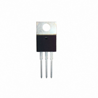
... V 20V 1 78dB o f=120Hz 2.0V I =1.0A 17mohm f=1.0KHz o 750mA T = 2. 125 C, o 1.1mV =5mA MC7805CT Three-Terminal Positive Voltage Regulators TO-220 PIN 1. o =25 C PIN 2. j PIN DIMENSIONS INCHES DIM MIN MAX A .560 .625 B .380 .420 C .140 ...
Page 2
... MC7805CT Representation Schematic Diagram www.mccsemi.com Revision Micro Commercial Components 2011/01/01 ...
Page 3
... MCC's products are not authorized for use as critical components in life support devices or systems without the express written Counterfeiting of semiconductor parts is a growing problem in the industry. Micro Commercial Components (MCC) is taking strong measures to protect ourselves and our customers from the proliferation of counterfeit parts. MCC strongly encourages customers to purchase MCC parts either directly from MCC or from Authorized MCC Distributors who are listed by country on our web page cited below ...