MC79M12CDTRKG ON Semiconductor, MC79M12CDTRKG Datasheet - Page 2
MC79M12CDTRKG
Manufacturer Part Number
MC79M12CDTRKG
Description
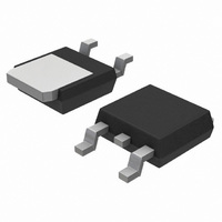
IC REG VOLT NEG 500MA 12V DPAK
Manufacturer
ON Semiconductor
Datasheet
1.MC79M05CDTRKG.pdf
(8 pages)
Specifications of MC79M12CDTRKG
Regulator Topology
Negative Fixed
Voltage - Output
-12V
Voltage - Input
Down to -35V
Voltage - Dropout (typical)
1.1V @ 500mA
Number Of Regulators
1
Current - Output
500mA
Operating Temperature
0°C ~ 125°C
Mounting Type
Surface Mount
Package / Case
TO-252-2, DPak (2 Leads + Tab), TO-252AA, SC-63
Polarity
Negative
Number Of Outputs
1
Output Type
Fixed
Output Voltage
- 12 V
Output Current
0.5 A
Line Regulation
80 mV
Load Regulation
240 mV
Dropout Voltage (max)
1.1 V
Input Voltage Max
- 35 V
Maximum Operating Temperature
+ 125 C
Minimum Operating Temperature
0 C
Mounting Style
SMD/SMT
Operating Temperature Range
0 C to + 125 C
Output Voltage Tolerance
4 %
Voltage Regulation Accuracy
4 %
Lead Free Status / RoHS Status
Lead free / RoHS Compliant
Current - Limit (min)
-
Lead Free Status / Rohs Status
Lead free / RoHS Compliant
Other names
MC79M12CDTRKGOS
MC79M12CDTRKGOS
MC79M12CDTRKGOSTR
MC79M12CDTRKGOS
MC79M12CDTRKGOSTR
Available stocks
Company
Part Number
Manufacturer
Quantity
Price
Company:

Part Number:
MC79M12CDTRKG
Manufacturer:
ROHM
Quantity:
60 000
Part Number:
MC79M12CDTRKG
Manufacturer:
ON/安森美
Quantity:
20 000


Stresses exceeding Maximum Ratings may damage the device. Maximum Ratings are stress ratings only. Functional operation above the
Recommended Operating Conditions is not implied. Extended exposure to stresses above the Recommended Operating Conditions may affect
device reliability.
*This device series contains ESD protection and exceeds the following tests:
MAXIMUM RATINGS
MC79M05B, C
ELECTRICAL CHARACTERISTICS
1. Load and line regulation are specified at constant temperature. Change in V
2. B = T
Input Voltage
Power Dissipation
Storage Junction Temperature
Operating Junction Temperature Range
Output Voltage (T
Line Regulation, T
Load Regulation, T
Output Voltage
Input Bias Current (T
Input Bias Current Change
Output Noise Voltage, T
Ripple Rejection (f = 120 Hz)
Dropout Voltage
Average Temperature Coefficient of Output Voltage
Human Body Model 2000 V per MIL_STD_883, Method 3015
Machine Model Method 200 V
Case 221A (TO−220−3)
Case 369C (DPAK−3)
Pulse testing with low duty cycle is used.
T
Thermal Resistance, Junction−to−Ambient
Thermal Resistance, Junction−to−Case
T
Thermal Resistance, Junction−to−Ambient
Thermal Resistance, Junction−to−Case
A
A
= 25°C
= 25°C
low
−7.0 Vdc ≥ V
−8.0 Vdc ≥ V
5.0 mA ≤ I
−7.0 Vdc ≥ V
−8.0 Vdc ≥ V
5.0 mA ≤ I
I
I
O
O
to T
= 500 mA, T
= 5.0 mA, 0°C ≤ T
high
J
J
J
= 25°C)
, −40°C < T
= 25°C (Note 1)
O
O
= 25°C (Note 1)
J
≤ 500 mA
= 25°C)
≤ 350 mA, V
I
I
I
I
A
≥ −25 Vdc
≥ −18 Vdc
≥ −25 Vdc, 5.0 mA ≤ I
≥ −25 Vdc, I
(T
J
= 25°C, 10 Hz ≤ f ≤ 100 kHz
= 25°C
A
= 25°C, unless otherwise noted.)
J
J
< 125°C C = T
≤ 125°C
Characteristic
I
= −10 V
O
= 350 mA
(V
Rating
I
= −10 V, I
O
low
≤ 350 mA
to T
high
O
= 350 mA, T
http://onsemi.com
, 0°C < T
J
2
< 125°C.
low
to T
high
O
due to heating effects must be taken into account separately.
(Note 2), unless otherwise noted.)
Symbol
DV
Reg
Reg
V
DI
RR
V
V
I
I
V
−V
O
IB
O
O
load
IB
n
/DT
line
O
Symbol
q
q
q
q
T
−4.75
P
P
V
T
−4.8
JC
JC
stg
Min
JA
JA
D
D
54
J
I
−
−
−
−
−
−
−
−
−
Internally Limited
Internally Limited
−5.0
Typ
7.0
2.0
4.3
1.1
0.2
30
40
66
−65 to +150
−40 to +150
−
−
−
Value
−35
5.0
6.0
65
92
−5.25
Max
−5.2
100
8.0
0.4
0.4
50
30
−
−
−
−
mV/°C
°C/W
°C/W
°C/W
°C/W
Unit
Vdc
Unit
Vdc
Vdc
Vdc
mV
mV
mA
mA
°C
°C
dB
W
W
mV
Related parts for MC79M12CDTRKG
Image
Part Number
Description
Manufacturer
Datasheet
Request
R

Part Number:
Description:
ON Semiconductor [VOLTAGE REGULATOR]
Manufacturer:
ON Semiconductor
Datasheet:
Part Number:
Description:
357-036-542-201 CARDEDGE 36POS DL .156 BLK LOPRO
Manufacturer:
ON Semiconductor
Datasheet:
Part Number:
Description:
357-036-542-201 CARDEDGE 36POS DL .156 BLK LOPRO
Manufacturer:
ON Semiconductor
Datasheet:
Part Number:
Description:
357-036-542-201 CARDEDGE 36POS DL .156 BLK LOPRO
Manufacturer:
ON Semiconductor
Datasheet:
Part Number:
Description:
357-036-542-201 CARDEDGE 36POS DL .156 BLK LOPRO
Manufacturer:
ON Semiconductor
Datasheet:
Part Number:
Description:
357-036-542-201 CARDEDGE 36POS DL .156 BLK LOPRO
Manufacturer:
ON Semiconductor
Datasheet:
Part Number:
Description:
357-036-542-201 CARDEDGE 36POS DL .156 BLK LOPRO
Manufacturer:
ON Semiconductor
Datasheet:
Part Number:
Description:
357-036-542-201 CARDEDGE 36POS DL .156 BLK LOPRO
Manufacturer:
ON Semiconductor
Datasheet:
Part Number:
Description:
357-036-542-201 CARDEDGE 36POS DL .156 BLK LOPRO
Manufacturer:
ON Semiconductor
Datasheet:
Part Number:
Description:
357-036-542-201 CARDEDGE 36POS DL .156 BLK LOPRO
Manufacturer:
ON Semiconductor
Datasheet:
Part Number:
Description:
357-036-542-201 CARDEDGE 36POS DL .156 BLK LOPRO
Manufacturer:
ON Semiconductor
Datasheet:
Part Number:
Description:
Manufacturer:
ON Semiconductor
Datasheet:
Part Number:
Description:
Manufacturer:
ON Semiconductor
Datasheet:
Part Number:
Description:
Manufacturer:
ON Semiconductor
Datasheet: