MCP1825T-3302E/DC Microchip Technology, MCP1825T-3302E/DC Datasheet
MCP1825T-3302E/DC
Specifications of MCP1825T-3302E/DC
Available stocks


Related parts for MCP1825T-3302E/DC


MCP1825T-3302E/DC Summary of contents
Page 1
... Notebook Computers • Network Interface Cards • Palmtop Computers • 2.5V to 1.XV Regulators © 2008 Microchip Technology Inc. Description The MCP1825/MCP1825S is a 500 mA Low Dropout (LDO) linear regulator that provides high current and low output voltages. The MCP1825 comes in a fixed or adjustable output voltage version, with an output voltage range of 0 ...
Page 2
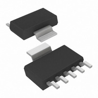
... Package Types MCP1825 DDPAK-5 Fixed/Adjustable SOT-223 Pin Fixed 1 SHDN GND (TAB OUT 5 PWRGD 6 GND (TAB) DS22056B-page 2 TO-220-5 DDPAK Adjustable SHDN V IN GND (TAB) V OUT ADJ GND (TAB) MCP1825S TO-220 SOT-223 Pin GND (TAB OUT 4 GND (TAB) © 2008 Microchip Technology Inc. ...
Page 3
... Typical Applications On SHDN Off V = 2. 4.7 µF On SHDN Off 2. 4.7 µF © 2008 Microchip Technology Inc. MCP1825/MCP1825S MCP1825 Fixed Output Voltage R 1 100 kΩ OUT GND MCP1825 Adjustable Output Voltage V ADJ R 40 kΩ OUT GND PWRGD V = 1.8V @ 500 mA ...
Page 4
... MCP1825/MCP1825S Functional Block Diagram - Adjustable Output V IN Undervoltage Lock Out (UVLO) SHDN Overtemperature Sensing V IN SHDN Soft-Start GND DS22056B-page 4 PMOS I SNS Driver w/limit EA and SHDN – SHDN V REF Reference Comp 92 REF V OUT ADJ/SENSE T DELAY © 2008 Microchip Technology Inc. ...
Page 5
... Functional Block Diagram - Fixed Output (3-Pin Undervoltage Lock Out (UVLO) SHDN Overtemperature Sensing V IN SHDN Soft-Start GND © 2008 Microchip Technology Inc. MCP1825/MCP1825S PMOS I SNS Driver w/limit EA and SHDN – SHDN V REF Reference Comp 92 REF V OUT Sense T DELAY DS22056B-page 5 ...
Page 6
... MCP1825/MCP1825S Functional Block Diagram - Fixed Output (5-Pin Undervoltage Lock Out (UVLO) SHDN Overtemperature Sensing V IN SHDN Soft-Start GND DS22056B-page 6 PMOS I SNS Driver w/limit EA and SHDN – SHDN V REF Reference Comp 92 REF V OUT Sense PWRGD T DELAY © 2008 Microchip Technology Inc. ...
Page 7
... The junction temperature is approximated by soaking the device under test at an ambient temperature equal to the desired junction temperature. The test time is small enough such that the rise in the junction temperature over the ambient temperature is not significant. © 2008 Microchip Technology Inc. MCP1825/MCP1825S † Notice: Stresses above those listed under “Maximum Rat- ings” ...
Page 8
... SHDN = GND GND to 95% V OUT R µV/√ 200 mA kHz, OUT µF (X7R Ceramic), OUT V = 2.5V OUT + V DROPOUT(MAX). is the desired set point output R is the highest voltage measured over the + V . DROPOUT(MAX) ). Exceeding the maximum allowable power © 2008 Microchip Technology Inc. ...
Page 9
... The junction temperature is approximated by soaking the device under test at an ambient temperature equal to the desired junction temperature. The test time is small enough such that the rise in the junction temperature over the ambient temperature is not significant. © 2008 Microchip Technology Inc. MCP1825/MCP1825S = V ...
Page 10
... Steady State °C Transient °C °C/W 4-Layer JC51 Standard Board °C/W 4-Layer JC51 Standard Board °C/W EIA/JEDEC JESD51-751-7 4 Layer Board °C/W 4-Layer JC51 Standard Board °C/W 4-Layer JC51 Standard Board °C/W EIA/JEDEC JESD51-751-7 4 Layer Board © 2008 Microchip Technology Inc. ...
Page 11
... V =3.0V V =2. -45 - Temperature (°C) FIGURE 2-3: Quiescent Current vs. Junction Temperature (Adjustable Version). © 2008 Microchip Technology Inc. MCP1825/MCP1825S = 4.7 µF Ceramic (X7R 4.7 µF Ceramic (X7R 0.10 0.09 0.08 0.07 0.06 0.05 0.04 0.03 0.02 0.01 0. -45 FIGURE 2-4: Temperature (Adjustable Version) ...
Page 12
... OUT OUT +130°C +90°C +25°C +0°C -45°C 3.5 4 4.5 5 5.5 6 Input Voltage (V) Quiescent Current vs. Input V = 2.3V for V =0. 3.0V for V =2. =2.5V =0.8V 100 200 300 400 500 600 Load Current (mA) Ground Current vs. Load © 2008 Microchip Technology Inc. ...
Page 13
... OUT 0.05 0. 250 mA OUT 0. 500 mA OUT 0.02 -45 - Temperature (°C) FIGURE 2-15: Line Regulation vs. Temperature. © 2008 Microchip Technology Inc. MCP1825/MCP1825S = 4.7 µF Ceramic (X7R 4.7 µF Ceramic (X7R 0.045 0.040 I OUT 0.035 I OUT 0.030 0.025 0.020 I OUT 0.015 105 130 -45 FIGURE 2-16: Temperature ...
Page 14
... Output Noise Voltage V =1.2V Adj R C =10 μF ceramic X7R OUT V =2. μ =10 mA OUT 0 100 1000 Frequency (kHz) Power Supply Ripple V =2.5V (Fixed =22 μF ceramic X7R OUT V =3. μ =10 mA OUT 0 100 1000 Frequency (kHz) Power Supply Ripple © 2008 Microchip Technology Inc. ...
Page 15
... IN OUT FIGURE 2-25: 2.5V (Adj.) Startup from V FIGURE 2-26: 2.5V (Adj.) Startup from Shutdown. FIGURE 2-27: Power Good (PWRGD) Timing. © 2008 Microchip Technology Inc. MCP1825/MCP1825S = 4.7 µF Ceramic (X7R 4.7 µF Ceramic (X7R FIGURE 2-28: IN FIGURE 2-29 500 mA). FIGURE 2-30: ( 500 mA) ...
Page 16
... The DDPAK and TO-220 package have an exposed tab on the package. A heat sink may may be mount to the tab to aid in the removal of heat from the package during operation. The exposed tab is at the ground potential of the LDO. ) OUT © 2008 Microchip Technology Inc. ...
Page 17
... GND 4.7 µF FIGURE 4-1: Typical adjustable output voltage application circuit. The allowable resistance value range for resistor R from 10 kΩ to 200 kΩ. Solving the equation for R yields the following equation: © 2008 Microchip Technology Inc. MCP1825/MCP1825S EQUATION 4-2: R Where OUT ...
Page 18
... LDO will enter Shutdown mode. This small bit of filtering helps to reject any system noise spikes on the shutdown input signal. < 0.4V maximum). TPG VOH TVDET_PWRG VOL Power Good Timing µ Power Good Timing from , with minimum IN © 2008 Microchip Technology Inc. ...
Page 19
... SHDN V OUT FIGURE 4-4: Shutdown Input Timing Diagram. © 2008 Microchip Technology Inc. MCP1825/MCP1825S 4.7 Dropout Voltage and Undervoltage Lockout Dropout voltage is defined as the input-to-output voltage differential at which the output voltage drops 2% below the nominal value that was measured with ...
Page 20
... Because of the GND for the MCP1825/ GND IN continuous operating junction ) of the device. The thermal JA × Rθ TOTAL JA AMAX = Maximum continuous junction temperature = Total device power dissipation = Thermal resistance from junction to ambient = Maximum ambient temperature © 2008 Microchip Technology Inc. of ...
Page 21
... T = Rise in device junction temperature J(RISE) over the ambient temperature T = Ambient temperature A © 2008 Microchip Technology Inc. MCP1825/MCP1825S 5.3 Typical Application Internal power dissipation, junction temperature rise, junction temperature and maximum power dissipation is calculated in the following example. The power dissipation as a result of ground current is small enough to be neglected ...
Page 22
... D(MAX) DDPAK-5 (31.2°C/Watt Rθ (125°C – 60°C)/ 31.2°C/W D(MAX 2.083W D(MAX) From this table, you can see the difference in maximum allowable power dissipation between the TO-220-5 package and the DDPAK-5 package. DS22056B-page 22 © 2008 Microchip Technology Inc. ...
Page 23
... Note: In the event the full Microchip part number cannot be marked on one line, it will be carried over to the next line, thus limiting the number of available characters for customer-specific information. © 2008 Microchip Technology Inc. MCP1825/MCP1825S Example: MCP1825S e ...
Page 24
... In the event the full Microchip part number cannot be marked on one line, it will be carried over to the next line, thus limiting the number of available characters for customer-specific information. DS22056B-page 24 Example: MCP1825 e 3 12EET 0710256 Example: 1825-08 EDC0710 256 Example: MCP1825 e 3 08EAT^^ 0710256 © 2008 Microchip Technology Inc. ...
Page 25
... Significant Characteristic. 2. Dimensions D and E do not include mold flash or protrusions. Mold flash or protrusions shall not exceed .005" per side. 3. Dimensioning and tolerancing per ASME Y14.5M. BSC: Basic Dimension. Theoretically exact value shown without tolerances. © 2008 Microchip Technology Inc. MCP1825/MCP1825S E1 L1 ...
Page 26
... D 6.30 c 0.23 b 0.60 b2 2.90 L 0.75 φ 0° c NOM MAX 3 – 1.80 – 0.10 1.60 1.70 7.00 7.30 3.50 3.70 6.50 6.70 0.30 0.35 0.76 0.84 3.00 3.10 – – – 10° Microchip Technology Drawing C04-032B © 2008 Microchip Technology Inc. ...
Page 27
... Microchip Technology Inc. MCP1825/MCP1825S DS22056B-page 27 ...
Page 28
... NOM MAX 3 – .190 – .055 – .115 – .420 – .120 – .650 – .355 – .270 – .156 – .580 – .250 – .024 .027 .040 .057 .070 Microchip Technology Drawing C04-034B © 2008 Microchip Technology Inc. ...
Page 29
... Significant Characteristic. 2. Dimensions D and E do not include mold flash or protrusions. Mold flash or protrusions shall not exceed .005" per side. 3. Dimensioning and tolerancing per ASME Y14.5M. BSC: Basic Dimension. Theoretically exact value shown without tolerances. © 2008 Microchip Technology Inc. MCP1825/MCP1825S E1 L1 ...
Page 30
... MCP1825/MCP1825S DS22056B-page φ © 2008 Microchip Technology Inc. ...
Page 31
... Microchip Technology Inc. MCP1825/MCP1825S DS22056B-page 31 ...
Page 32
... INCHES NOM MAX 5 .067 BSC .268 BSC – .190 – .420 – .650 – .355 – .293 – .055 – .120 – .156 – .590 – .115 – .025 .027 .040 Microchip Technology Drawing C04-036B © 2008 Microchip Technology Inc. ...
Page 33
... Updated Figure 2-4, Figure 2-5, Figure 2-16, Figure 2-29, and Figure 2-30. 2. Updated package outline drawings and landing pattern drawings to Section 6.0 “Packaging Information”. Updated Appendix A: “Revision History”. 3. Revision A (August 2007) • Original Release of this Document. © 2008 Microchip Technology Inc. MCP1825/MCP1825S DS22056B-page 33 ...
Page 34
... MCP1825/MCP1825S NOTES: DS22056B-page 34 © 2008 Microchip Technology Inc. ...
Page 35
... X Device Output Feature Tolerance Voltage Code Device: MCP1825: 500 mA Low Dropout Regulator MCP1825T: 500 mA Low Dropout Regulator Tape and Reel MCP1825S: 500 mA Low Dropout Regulator MCP1825ST: 500 mA Low Dropout Regulator Tape and Reel Output Voltage *: 08 = 0.8V “Standard” 1.2V “Standard” ...
Page 36
... MCP1825/MCP1825S NOTES: DS22056B-page 36 © 2008 Microchip Technology Inc. ...
Page 37
... PowerMate, PowerTool, REAL ICE, rfLAB, Select Mode, Total Endurance, UNI/O, WiperLock and ZENA are trademarks of Microchip Technology Incorporated in the U.S.A. and other countries. SQTP is a service mark of Microchip Technology Incorporated in the U.S.A. All other trademarks mentioned herein are property of their respective companies. ...
Page 38
... Fax: 886-3-572-6459 Taiwan - Kaohsiung Tel: 886-7-536-4818 Fax: 886-7-536-4803 Taiwan - Taipei Tel: 886-2-2500-6610 Fax: 886-2-2508-0102 Thailand - Bangkok Tel: 66-2-694-1351 Fax: 66-2-694-1350 © 2008 Microchip Technology Inc. EUROPE Austria - Wels Tel: 43-7242-2244-39 Fax: 43-7242-2244-393 Denmark - Copenhagen Tel: 45-4450-2828 Fax: 45-4485-2829 France - Paris Tel: 33-1-69-53-63-20 ...