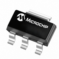
MCP1790-3302E/DB Microchip Technology, MCP1790-3302E/DB Datasheet - Page 17

MCP1790-3302E/DB
Manufacturer Part Number
MCP1790-3302E/DB
Description
IC LDO REG 70MA 3.3V SOT-223-3
Manufacturer
Microchip Technology
Datasheet
1.MCP1791T-3302EDC.pdf
(34 pages)
Specifications of MCP1790-3302E/DB
Package / Case
SOT-223 (3 leads + Tab), SC-73, TO-261
Regulator Topology
Positive Fixed
Voltage - Output
3.3V
Voltage - Input
6 ~ 30 V
Voltage - Dropout (typical)
0.7V @ 70mA
Number Of Regulators
1
Current - Output
70mA (Min)
Operating Temperature
-40°C ~ 125°C
Mounting Type
Surface Mount
Number Of Outputs
1
Polarity
Positive
Input Voltage Max
30 V
Output Voltage
3.3 V
Output Type
Fixed
Dropout Voltage (max)
1.3 V at 70 mA
Output Current
70 mA
Line Regulation
+/- 0.0002 % / V
Load Regulation
+/- 0.2 %
Voltage Regulation Accuracy
2.5 %
Maximum Operating Temperature
+ 125 C
Mounting Style
SMD/SMT
Minimum Operating Temperature
- 40 C
Lead Free Status / RoHS Status
Lead free / RoHS Compliant
Current - Limit (min)
-
Lead Free Status / Rohs Status
Lead free / RoHS Compliant
Available stocks
Company
Part Number
Manufacturer
Quantity
Price
Company:
Part Number:
MCP1790-3302E/DB
Manufacturer:
MICROCHIP
Quantity:
12 000
4.9
The MCP1791 has an open-drain Power Good
(PWRGD) output signal capable of sinking a minimum
of 5.0 mA of current while maintaining a PWRGD
output voltage of 0.4V or less.
As the output voltage of the LDO rises, the PWRGD
output will be held low until the output voltage has
exceeded the power good threshold (V
by an amount equal to the power good hysteresis value
((V
has been exceeded, the power good output signal will
be pulled high by an external pull-up resistor, indicating
that the output voltage is stable and within regulation
limits.
If the output voltage of the LDO falls below the power
good threshold (V
output will transition low. The power good circuitry has
a 235 µs delay when detecting a falling output voltage,
which helps to increase noise immunity of the power
good output and avoid false triggering of the power
good output during fast output transients. See
Figure 4-4
When the LDO is put into Shutdown mode using the
SHDN input, the power good output is pulled low within
400 ns typical, indicating that the output voltage will be
out of regulation. The timing diagram for the power
good output when using the shutdown input is shown in
Figure
The PWRGD output may be pulled up to either V
V
sink very little current during shutdown. When PWRGD
is pulled up to V
during shutdown. That is because V
shutdown while V
output is pulled to V
track V
circuitry has been reached and the PWRGD circuitry
pulls the signal back low. Therefore, when pulling
PWRGD to VIN instead of V
aware of the PWRGD signal going high while the input
voltage is rising at startup. Pulling PWRGD to V
removes the startup pulse.
© 2008 Microchip Technology Inc.
OUT
PWRGD_HYS
. When pulled to V
4-5.
IN
Power Good Output (PWRGD)
at startup until the threshold of the PWRGD
for power good timing characteristics.
), typically 2% of V
IN
IN
, the PWRGD output will sink current
PWRGD_TH
IN
is still active. When the PWRGD
, the PWRGD output signal will
OUT
OUT
, the PWRGD output will
) level, the power good
, the designer must be
R
. Once this threshold
PWRGD_TH
OUT
is 0 during
) level
IN
OUT
or
FIGURE 4-4:
FIGURE 4-5:
Shutdown.
V
PWRGD
V
V
SHDN
MCP1790/MCP1791
IN
PWRGD_TH
OUT
V
100 µs
PWRGD
OUT
T
30 µs
OR
T
100 µs
PG
C
LOAD
Power Good Timing.
Power Good Timing from
V
OH
V
= 1.0 µF
PWRGD_HYS
T
PG
DS22075A-page 17
T
V
VDET_PWRGD
OL
235 µs


