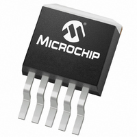
TC1265-2.5VETTR Microchip Technology, TC1265-2.5VETTR Datasheet - Page 7

TC1265-2.5VETTR
Manufacturer Part Number
TC1265-2.5VETTR
Description
IC REG LDO 2.5V 800MA SD DDPAK-5
Manufacturer
Microchip Technology
Specifications of TC1265-2.5VETTR
Regulator Topology
Positive Fixed
Voltage - Output
2.5V
Voltage - Input
Up to 6V
Voltage - Dropout (typical)
1.2V @ 800mA
Number Of Regulators
1
Current - Output
800mA (Min)
Operating Temperature
-40°C ~ 125°C
Mounting Type
Surface Mount
Package / Case
TO-263-5, D²Pak (5 leads + Tab), TO-263BA
Number Of Outputs
1
Polarity
Positive
Input Voltage Max
6 V
Output Voltage
2.5 V
Output Type
Fixed
Dropout Voltage (max)
1400 mV
Output Current
800 mA
Line Regulation
0.001 %
Load Regulation
0.002 % / mA
Voltage Regulation Accuracy
0.5 %
Maximum Operating Temperature
+ 125 C
Mounting Style
SMD/SMT
Minimum Operating Temperature
- 40 C
Lead Free Status / RoHS Status
Lead free / RoHS Compliant
Current - Limit (min)
-
Lead Free Status / Rohs Status
Lead free / RoHS Compliant
Other names
TC126525VETTR
4.0
The TC1265 is a precision, fixed-output LDO. Unlike
bipolar regulators, the TC1265’s supply current does
not increase with load current. In addition, V
remains stable and within regulation over the entire
0 mA to I
consideration in RTC and CMOS RAM battery back-up
applications).
Figure 4-1 shows a typical application circuit.
FIGURE 4-1:
4.1
A 1 µF (min.) capacitor from V
required. The output capacitor should have an Effective
Series Resistance (ESR) greater than 0.1
than 5 . A 1 µF capacitor should be connected from
V
between the regulator and the AC filter capacitor, or if a
battery is used as the power source. Aluminum electro-
lytic or tantalum capacitor types can be used. Since
many aluminum electrolytic capacitors freeze at
approximately -30°C, solid tantalums are recom-
mended for applications operating below -25°C. When
operating from sources other than batteries, supply-
noise rejection and transient response can be
improved by increasing the value of the input and
output capacitors, and by employing passive filtering
techniques.
2004 Microchip Technology Inc.
Shutdown Control
(to CMOS Logic or Tie
to V
IN
IN
to GND if there is more than 10 inches of wire
, if unused)
+
DETAILED DESCRIPTION
Battery
Output Capacitor
LOADMAX
+
1 µF
C
1
Processor RESET Signal
if ERROR is used as a
C
GND
load current range (an important
SHDN
V
3
IN
Required Only
(See Text)
TC1265
Typical Application Circuit.
ERROR
V
OUT
OUT
+
V
1 µF
C
+
+
2
0.2 µF
C
to ground is
R
1 M
3
1
V
and less
OUT
BATTLOW
or RESET
OUT
4.2
ERROR is driven low whenever V
regulation by more than – 5% (typ.). This condition may
be caused by low input voltage, output current limiting,
or thermal limiting. The ERROR threshold is 5% below
rated V
voltage value (e.g., ERROR = V
5.0V regulator and 2.85V (typ.) for a 3.0V regulator).
ERROR output operation is shown in Figure 4-2.
Note that ERROR is active when V
V
As shown in Figure 4-1, ERROR can be used as a
battery low flag or as a processor RESET signal (with
the addition of timing capacitor C
chosen to maintain ERROR below V
RESET input for at least 200 ms to allow time for the
system to stabilize. Pull-up resistor R
V
FIGURE 4-2:
ERROR
TH
OUT
V
V
OUT
V
V
and inactive when V
OL
, V
TH
IH
IN
OUT
ERROR Output
or any other voltage less than (V
regardless of the programmed output
ERROR Output Operation.
OUT
is above V
OL
3
). R
TC1265
at 4.75V (typ.) for a
OUT
IH
OUT
DS21376C-page 7
1
1
of the processor
x C
TH
can be tied to
is at or below
Hysteresis (V
falls out of
+ V
3
IN
should be
+ 0.3V).
H
.
H
)


